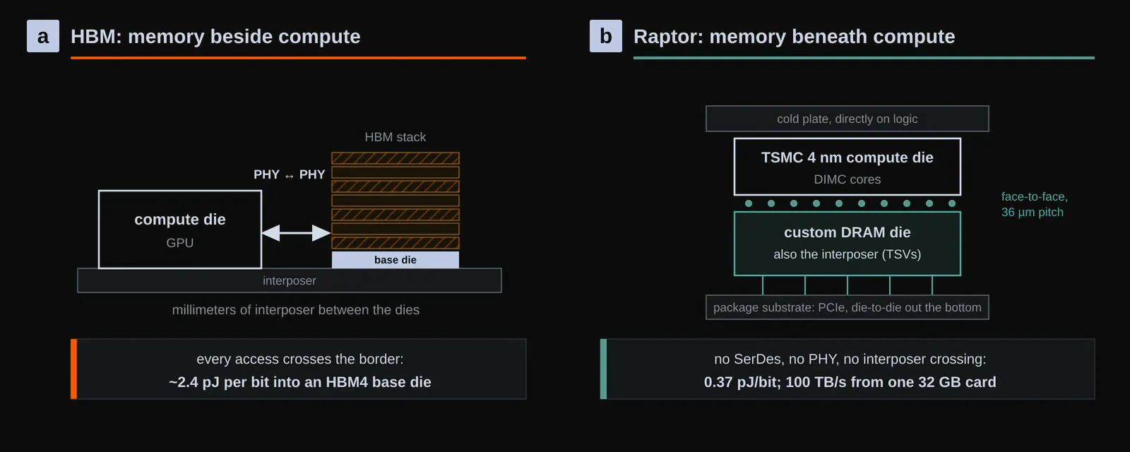
Every HBM system pays the same toll. The DRAM stack sits millimeters from the compute die, the two talk across an interposer through a PHY on each side, and moving one bit into an HBM4 base die costs roughly 2.4 pJ before any computation happens. The toll is not incidental: in token-by-token generation, where each output token requires streaming the active weights and KV state past the compute, memory traffic is the workload, and the interface energy scales with every byte of it. The ISCA 2026 paper on Raptor and the subsequent Hot Chips presentation describe a different route: bond a TSMC 4 nm compute die face to face onto custom DRAM and remove the long electrical interface[1][2]. At a 36 µm microbump pitch, the PHY disappears and the vertical interface moves bits at 0.37 pJ, about 6.5× less energy than the HBM4 path. The advertised product target is 100 TB/s of memory bandwidth from a single card. The number that requires explaining is the other one: that card carries 32 GB.
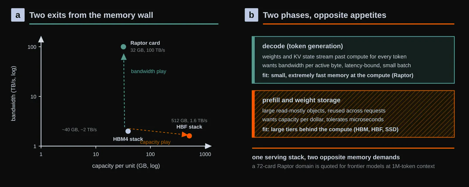
Coming three weeks after the HBF specification promised 512 GB stacks at HBM-class bandwidth, Raptor makes an instructive mirror image. The memory wall is being attacked from both ends at once: HBF trades latency for capacity, and Raptor trades capacity for bandwidth. We summarize the architecture, the packaging choices that make it work, and the scope of what has actually been demonstrated.
From SRAM to stacked DRAM
Raptor is the second act of an architecture d-Matrix has been building for years. Its shipping accelerator, Corsair, implements digital in-memory computing (DIMC): multiply-accumulate logic lives inside the memory arrays, so weights stay put and the compute comes to them. A Corsair chiplet packs 256 DIMC cores alongside 256 MB of SRAM[5], which delivers enormous bandwidth per byte but rations capacity in megabytes; models must shard across many chiplets, and SRAM’s cost per bit sets a hard ceiling on how far that scales. The obvious question was whether the same memory-side computing discipline could sit on a medium with DRAM’s density.
3DIMC is the answer, and it arrives with unusual provenance for a startup: a custom DRAM die co-developed with Alchip, announced in November 2025[4], and a dedicated test chip, Pavehawk, that validated the stacked DRAM-plus-logic combination in the lab before any product claim was made[5]. The ISCA paper adds something a product announcement cannot: it explains the mechanisms needed to make a wide, hot and densely banked DRAM stack reliable, then evaluates them across six generative workloads[1]. Hot Chips 2026 provides the complementary product view.
The stack is upside down
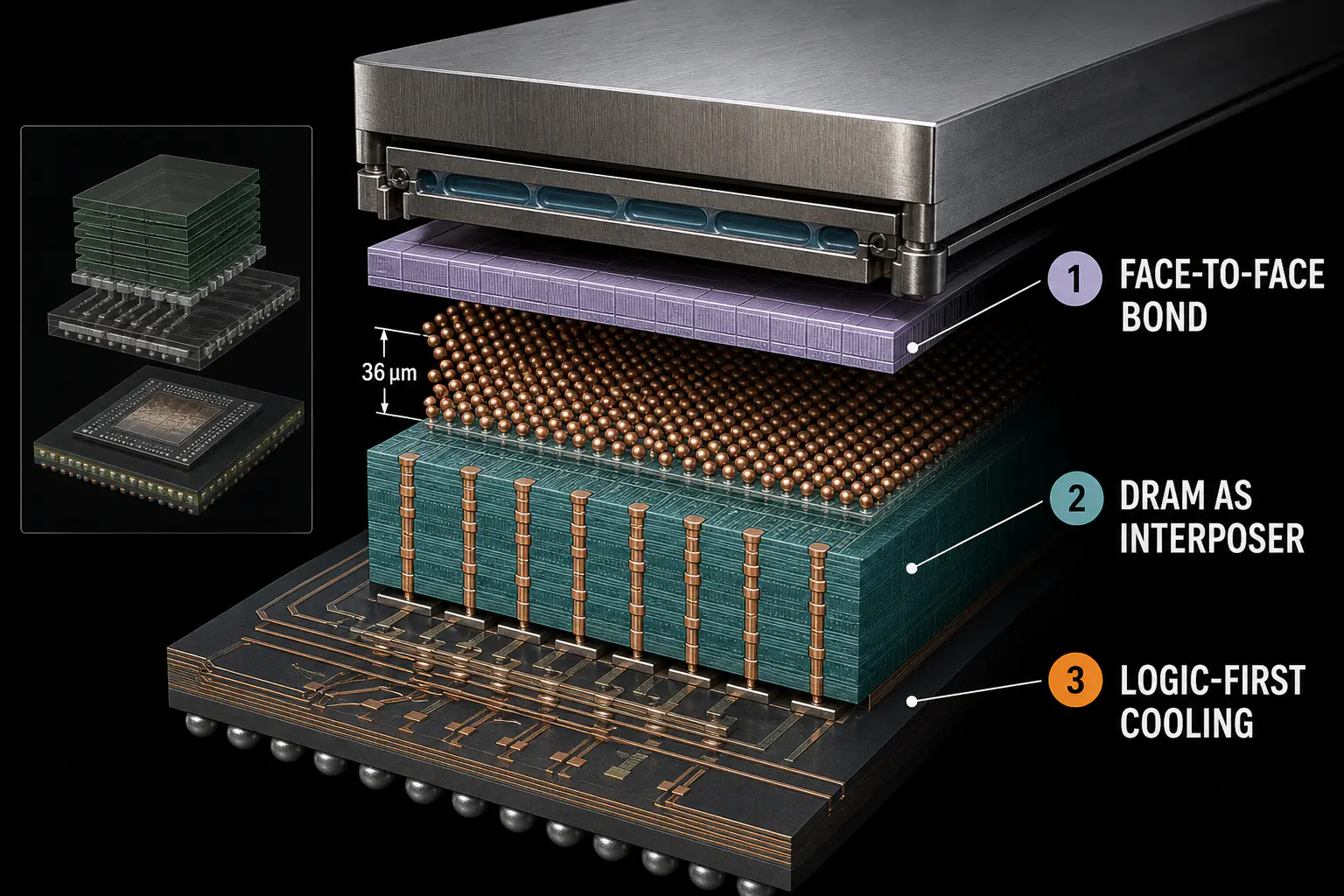
The packaging inverts the arrangement every HBM system uses, and each inversion has a reason. Logic goes on top: a liquid-cooling cold plate presses directly on the 4 nm compute die, instead of asking heat to escape through a thermally sensitive DRAM stack. DRAM goes underneath and moonlights as the interposer: PCIe and die-to-die signals travel down through the DRAM die’s TSVs to the package substrate, so the memory die is simultaneously storage and wiring[2][7]. Between the two dies there is no SerDes, no PHY and no interposer traversal, only a face-to-face microbump field at 36 µm pitch. Distance is what a PHY exists to overcome; remove the distance and the PHY, with its power and its latency, goes with it.
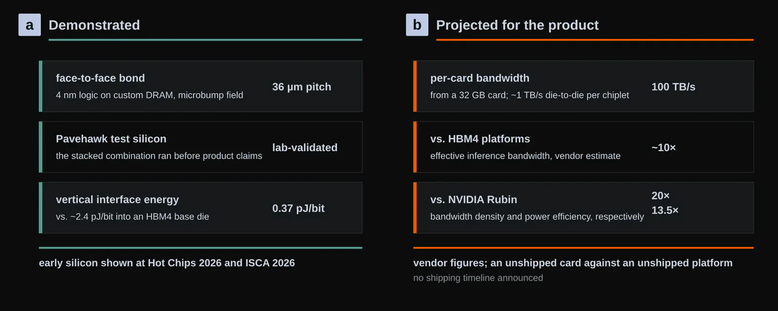
The claimed consequences compound. Per bit, the vertical interface costs 0.37 pJ against roughly 2.4 pJ for HBM4’s path. Per card, aggregate memory bandwidth reaches about 100 TB/s, a figure HBM systems reach only by summing eight or more stacks on the largest GPUs, and d-Matrix positions it as roughly 10× the effective inference bandwidth of HBM4-based platforms. Against NVIDIA’s Rubin generation, the company claims about 20× higher bandwidth density and 13.5× better power efficiency for the memory subsystem[7]. Note that these product-level comparisons remain vendor projections, not independent measurements of a shipping card.
The paper’s contribution is less photogenic but more important for judging whether the stack can operate. Stream-blocking maps KV-cache traffic onto a configurable number of 3D-DRAM channels instead of letting one workload shape dictate the physical layout. Pinless data-bus inversion reduces simultaneous switching on a single-cycle microbump interface without consuming extra package pins. Topology-preserving redundancy keeps the channel map intact when faulty resources are replaced, while temperature-aware refresh and interleaved ECC address the higher error pressure created by placing DRAM under logic. In plain language, bonding the dies solves distance, but creates mapping, power, fault and heat problems; the paper supplies one mechanism for each[1].
What 32 GB buys, and what it costs
A 32 GB card cannot hold a frontier model, and d-Matrix does not pretend otherwise. The deployment story is horizontal: the company describes a 72-card scale-up domain hosting a frontier-class model (its example is Kimi K3 at a 1M-token context), with each chiplet contributing about 1 TB/s of die-to-die bandwidth to hold the shards together[2]. The bet is that for latency-bound, small-batch token generation, the economics of many small, extremely fast memories beat the economics of few large, merely fast ones. This is precisely the opposite bet from HBF, which assumes the valuable working set is huge and read-mostly. Both can be right, because they target different phases of the same serving stack: decode wants bandwidth per active byte, and prefill plus weight storage wants capacity.
The honest caveats mirror the honest appeal. Capacity per card is 16× below an HBM4 GPU class device, so utilization depends on sharding software and on the interconnect between cards, the layer where, as our coverage of scale-up fabrics argued, determinism rather than raw bandwidth decides behavior at scale. Custom DRAM from a startup and a design-services partner enters a supply chain that HBM incumbents have spent a decade industrializing. Thermal headroom for the DRAM under a hot logic die is managed, not eliminated, by the inverted stack. Commercial availability and volume pricing have not been announced; the evidence available today is early silicon, a conference evaluation and forward-looking product specifications.
The claims, sorted by evidence
The evidence now falls into three levels. First, device evidence: Pavehawk validates the 3D bond and reports about 0.37 pJ/bit for the vertical interface. Second, paper evaluation: the workload set includes the speech models Whisper and Canary plus Llama 3.1 70B, DeepSeek-V3, Kimi K2 and GPT-OSS. Across that set, the ISCA study reports 4.71× higher throughput than its HBM configuration and 2.44× than its SRAM configuration, while also testing sensitivity to network latency and bandwidth[1]. These are comparisons within the paper’s modeled and early-silicon methodology, not measurements against retail GPU cards. Third, product projection: 100 TB/s per card, roughly 10× versus HBM4 platforms, and 20× bandwidth density with 13.5× power efficiency versus Rubin. The last group compares unshipped systems and should not be merged with the paper’s evaluation. This ordering is the same discipline we applied to the measured-silicon and calibrated-projection split in Panmnesia’s CXL switch paper.
What we take from it
We believe the durable insight here is architectural rather than competitive. For two decades the memory interface has been the negotiated border between two industries, and every negotiation produced a PHY. Raptor is the clearest demonstration yet that when one company controls both dies, the border can simply be abolished, and the 6.5× energy gap between 0.37 and 2.4 pJ/bit measures what the border was costing. Whether d-Matrix converts that into a business depends on software, supply chain and the interconnect questions above. However, the direction of travel is hard to unsee, and the incumbents have noticed: memory vendors are already moving logic into base dies and studying processing near memory. HBF widens the hierarchy’s floor; Raptor raises its ceiling. The AI memory system of the early 2030s increasingly looks like both at once, with HBM squeezed into the role of the middle tier, and the interesting engineering, as usual, in the software that decides which byte lives where.
The package trades PHY energy for thermal and yield constraints
Direct bonding removes much of the conventional DRAM interface path, but it also joins compute and memory more tightly in manufacturing and operation. A bad die, a bonding defect, or a thermal hotspot can affect the value of the complete stack. The economic question is therefore known-good-die yield and recoverable capacity after bonding, not only the performance of one successful package.
Thermal behavior deserves the same attention as bandwidth. Logic benefits from high power density and aggressive clocks, while DRAM retention and reliability prefer a cooler environment. Placing the tiers close shortens wires but couples their temperature. The package needs a measured map of junction temperature, memory temperature, throttling behavior, and sustained bandwidth under the intended inference duty cycle. A brief demonstration can reach a peak that a continuously serving module cannot maintain.
Repair and redundancy can soften yield loss. Spare memory regions, disabled compute tiles, or binning may recover partially functional stacks, but each changes advertised capacity and throughput. Buyers should ask how many package configurations are sold, what fraction of resources can be disabled, and whether software sees a uniform device. These details determine whether 3D integration improves total cost or concentrates failure into a more expensive unit.
Capacity should be measured at the model boundary
Thirty-two gigabytes of closely coupled DRAM changes which model state can remain beside compute, but it does not by itself say which models fit or how fast they run. Weight precision, KV-cache format, batch size, context length, activation workspace, and sparsity all compete for that capacity. The useful report maps each workload into weight bytes, dynamic state, temporary buffers, and remaining headroom.
The same map explains scale-out. A model that fits in one package avoids communication that a larger model must pay. Once multiple packages participate, the external fabric and partitioning strategy return to the critical path. Raptor’s local bandwidth can accelerate each shard while end-to-end throughput remains limited by expert routing, tensor collectives, or load imbalance. Package performance and system performance should therefore be reported separately.
Comparisons also need matched precision and quality. An accelerator can appear to fit a larger model by using a narrower format or more aggressive sparsity. That may be a valid product choice, but the result should state output quality, calibration, and any workload exclusions. Bytes saved by the algorithm are different from bytes supplied by the package.
Early silicon should lead to a qualification program
The paper’s strongest evidence is that the bonded concept exists in silicon. The next stage should establish repeatability across packages, workloads, and time. Qualification needs sustained inference, thermal cycling, memory error tracking, bonding reliability, and performance variation across samples. It should also include software recovery from corrected and uncorrected memory events, because a tightly integrated device cannot rely on replacing a conventional DIMM.
System trials should compare three boundaries: the same model on a conventional accelerator and external memory, one Raptor package when the model fits, and multiple packages when it does not. This separates the value of local 3D memory from the value of the compute architecture and from scale-out costs. Energy should be measured at the board or system input so removed PHY energy is not confused with a lower package-only number.
We read Raptor as a credible change in where the memory interface ends. Bonding compute to DRAM can turn interface energy and latency into package-design problems, which is valuable for generative inference with repeated weight and state access. The proof becomes a platform claim only after yield, sustained thermals, reliability, software behavior, and multi-package scaling are attached to the early-silicon result.
Source and attribution
This article is an editorial summary prepared for Silicon & Systems. Its primary technical source is the ISCA 2026 paper by Nair et al.; the Hot Chips presentation and public company materials provide product and packaging context. We restated the mechanisms, evaluation results and limitations in our own words. No source text, table, figure or slide is reproduced, and every figure on this page was created for this summary. The conference paper is (c) IEEE 2026; the presentation and company materials are (c) d-Matrix, Inc. 2026.