Five independent studies published between 2024 and 2025 place the round-trip latency of a one-hop commercial CXL memory expander between 265 and 442 ns[3][4]. Adding a switch raises that latency by roughly 2× because the request crosses at least two controller stacks plus a routing stage before reaching DRAM. The industry drew a practical conclusion. Hyperscalers deploy CXL over 1:1 direct links, use multi-headed devices (MHDs) when several hosts must share one enclosure, and in some cases argue that a memory pool obviates the switch entirely[5]. The measured latency of early products thus became a design assumption about CXL fabrics in general.
A paper presented at ISCA 2026 by Panmnesia argues that the assumption blames the wrong layer[1]. The protocol itself was engineered for memory semantics: fixed-size 256 B flits instead of PCIe’s variable-length packets, no completion round trips, a theoretical round-trip budget 4 to 10× below PCIe. What ships today, the authors contend, is protocol potential filtered through controller silicon inherited from PCIe IP libraries, which re-imports the layered pipelines, boundary buffering and host-centric routing that CXL was supposed to leave behind. Their answer is not another software layer but silicon: a unified controller that collapses the protocol stack into one pipeline, and a switch built around port-based routing (PBR) whose entire conversion and routing path runs in fixed-cycle hardware, fabricated in a 4 nm process. We summarize the argument in our own words below, and note where the evidence is measured silicon and where it is calibrated emulation. One disclosure up front: this paper comes from Panmnesia, where the editor of this site is CEO and a co-author, so read our enthusiasm with that in mind (details at the end).
Two routing modes and a transitional workaround
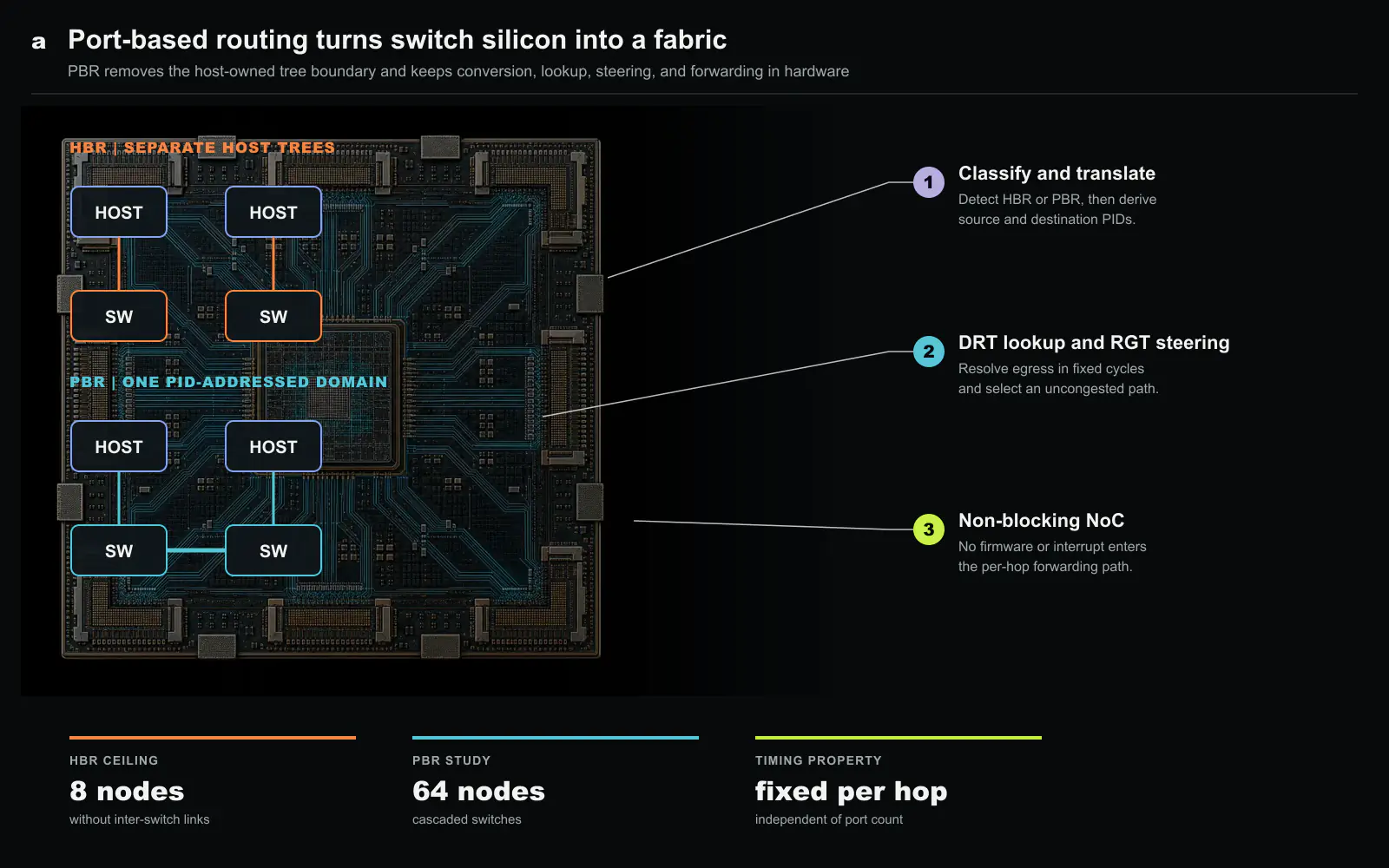
CXL inherits its scaling story from a fork the specification itself created. Hierarchy-based routing (HBR) mirrors the PCIe tree: each host owns a virtual switch containing its devices, address spaces stay per-host, and nothing is shared across the hierarchy. Port-based routing assigns every switch port a port ID (PID) and forwards by destination ID instead, so hosts, accelerators and memory devices sit in one flat fabric that a fabric manager maps into a global address and coherence domain. PBR is what makes switch cascading and arbitrary topologies possible, and it entered the standard with CXL 3.1[2]. However, nearly every controller and switch shipping in 2024 to 2025 still runs HBR only, and the paper measures the consequence: an HBR switch without inter-switch links tops out at 8 nodes on a 256-lane budget.
The industry’s interim answer, the MHD, packs several logical heads into one device so that several hosts can attach without a switch[6]. The paper is precise about why this remains a stopgap. Heads in practical devices number around four, since each head carries a full controller interface and die area is finite. Heads do not share a coherence domain, so data sharing across hosts falls back to software flushes or NUMA transactions. In addition, one device’s bandwidth divides among its active heads, so per-host bandwidth shrinks exactly when host count grows. Pooling capacity, in other words, is not the same thing as sharing data at hardware speed.
A controller with one clock and no seams
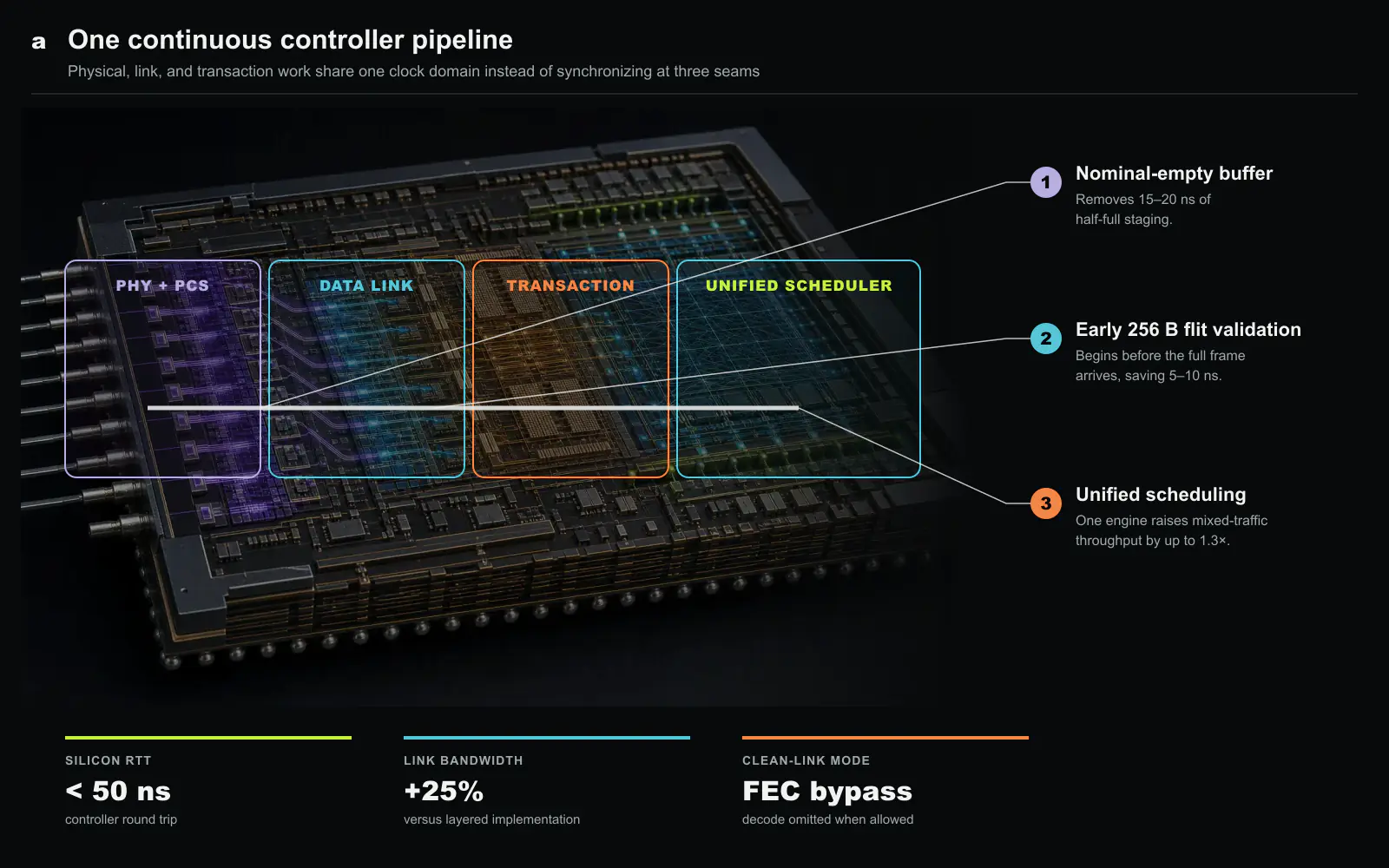
The paper’s first contribution addresses the controller stack itself. A conventional PCIe-derived controller couples three separately buffered pipelines: a physical layer (SerDes plus PCS), a data link layer for reliability, and a transaction layer for protocol semantics. Each boundary synchronizes neighboring layers through handshakes, so avoidable latency accumulates at the interfaces rather than on the wire. The proposed controller instead runs all three layers in a single clock domain under one timing reference, with shared buffering in place of interface staging.
The component savings are itemized rather than asserted. In the PCS, the conventional half-full elastic buffer that absorbs transmitter-receiver clock mismatch always imposes staging cycles; treating a nominally empty buffer as a valid state permits real-time clock alignment and recovers 15 to 20 ns on average. The link layer adopts a 256 B flit whose frame layout permits early validation of partial data, so the receiver starts processing before the full frame lands, worth another 5 to 10 ns over conventional 256 B flit designs. A forward error correction bypass engages when signal quality is high. Lastly, the transaction layer replaces per-protocol queues for CXL.io, CXL.cache and CXL.mem with one flow-control and scheduling engine, which lifts throughput by up to 1.3× under mixed traffic. With the layers fused, silicon evaluation puts controller round-trip latency below 50 ns, link bandwidth 25% higher, and latency variation under bursty load visibly tighter.
Routing as a pipeline stage, not a firmware call
The second contribution moves everything a switch does between ingress and egress into fixed-cycle hardware. Each port carries a classifier that identifies whether arriving traffic speaks HBR or PBR, conversion logic that derives source and destination PIDs and rewrites headers into the internal PBR format, and the reverse mapping for packets leaving toward legacy hosts. Forwarding then consults two hardware tables: a DPID routing table (DRT) that resolves the egress port with fixed-latency lookup, and a routing group table (RGT) that watches congestion across ports of equal reach and steers packets accordingly. Both tables accept lookups and updates concurrently, so topology changes and link recovery proceed without halting in-flight traffic, and a fabric-level timing mechanism keeps adjacent switches aligned for multi-hop operation.
Note that the design goal here is worded as determinism rather than raw speed. Because no firmware, interrupt or microcode scheduling sits anywhere in the path, every packet crosses the same pipeline stages in a bounded latency window, under congestion and across hops. That property is what the rest of the paper leans on: a fabric whose per-hop delay does not depend on port count, topology depth or a management core’s mood.
A switch built from port banks
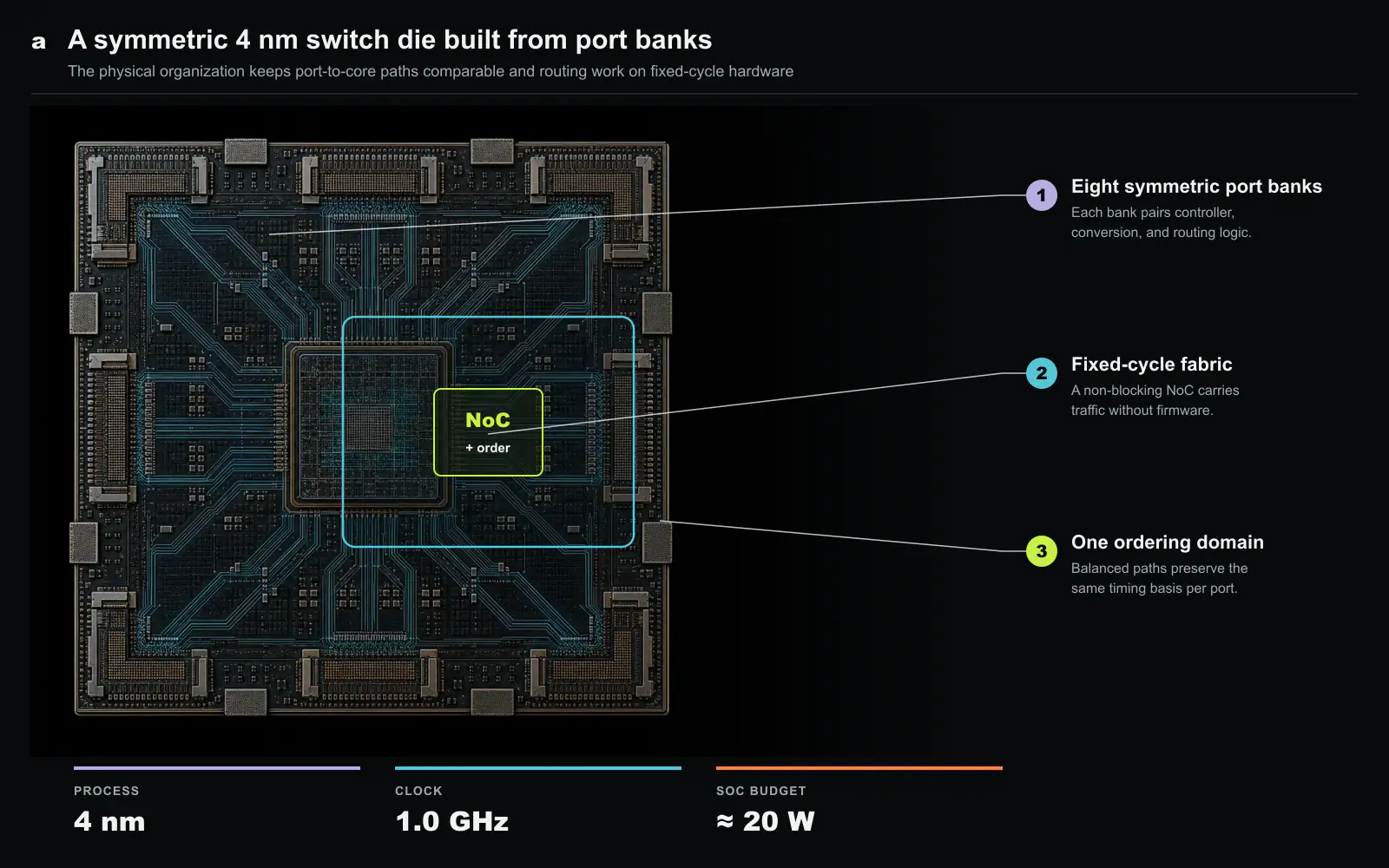
The third contribution assembles these parts into a fabric switch. The die is organized as port banks, each pairing a unified controller with its conversion and routing logic, interconnected by a non-blocking network-on-chip in a single timing domain; ports can merge into wide interfaces or split into narrow ones without changing latency behavior. Virtual CXL switch support spans single-root and multi-root configurations, with hardware dynamic-port binding allocating bandwidth and address space across hosts, and MHDs are supported as first-class citizens whose heads map to independent attachment points. The prototype is fabricated in a 4 nm process, clocks at 1.0 GHz, budgets roughly 20 W for the SoC, and drives 64 Gbps PAM4 SerDes, which places it on the PCIe 6.0 physical layer that CXL 3.2 requires. According to the paper, pre-release units of the switch are slated to reach customer sampling in the summer of 2026.
The sampling milestone has since occurred. In April 2026 Panmnesia started providing early-access partners with packaged pre-release parts of the productized design, marketed as a PCIe 6.4-CXL 3.2 fusion switch. The company’s announcement matches the paper’s architecture point for point: both routing modes coexist on one die (the PBR-HBR combination the port-bank classifier exists to serve), cascaded switches join devices across racks into a single fabric without falling back to Ethernet, and the attached population spans PCIe endpoints and CXL Type 1, Type 2 and Type 3 devices, with the proprietary controller holding double-digit nanosecond latency. The packaged parts below show that the per-port pipeline represented in the paper’s die micrograph has advanced to pre-release sampling.

What the numbers say
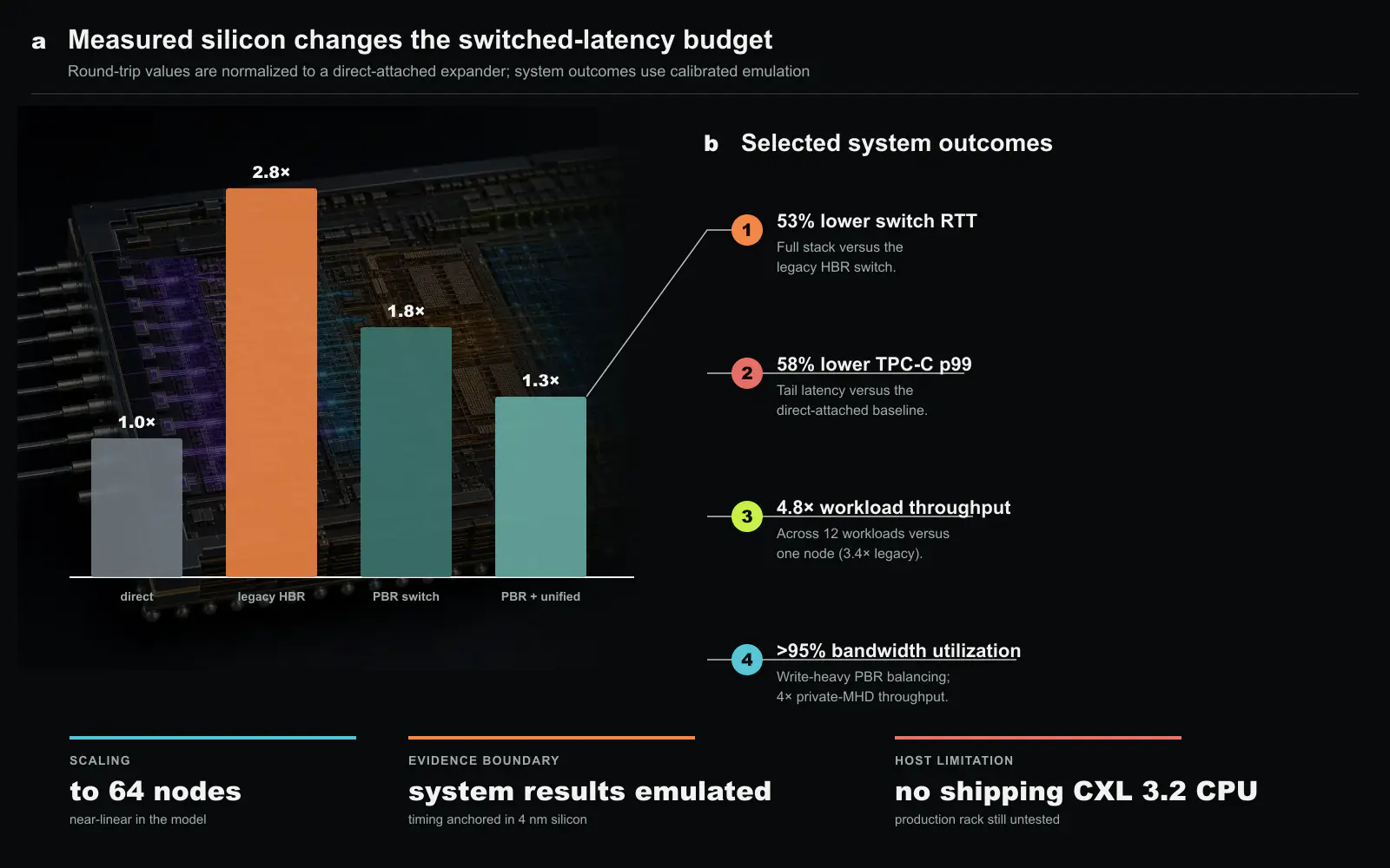
The evaluation platform deserves a careful read. The controller and the per-port pipeline exist as measured 4 nm silicon, with a die micrograph in the paper. The system-level numbers, however, come from cycle-accurate RTL emulation whose timing parameters (bus timing, pipeline depths) were extracted from that silicon and cross-checked against Memory Latency Checker data. The authors are direct about why: no shipping CPU exposes the PCIe 6.0 physical layer that CXL 3.2 needs, and CXL 2.0-era processors lack the full CXL.cache support that multi-host sharing tests require. The testbed models four 128-core nodes plus a 10 TB storage node running a distributed PostgreSQL 17, modified so that hardware coherence lets every node accept writes and reuse data cached by its peers.
The seven baselines are more informative than their abbreviated names first suggest. Four are direct-attached: one node with one single-headed device, four isolated node-device pairs, and one multi-headed device operated either as private heads or with software-maintained sharing. Three put four nodes and four devices behind a switch. The first retains a legacy HBR switch and controller, the second changes only the switch to PBR, and the last combines PBR with the unified controller. This sequence lets the evaluation separate the effect of sharing from the effect of switch routing and then from the cost of the controller pipeline.
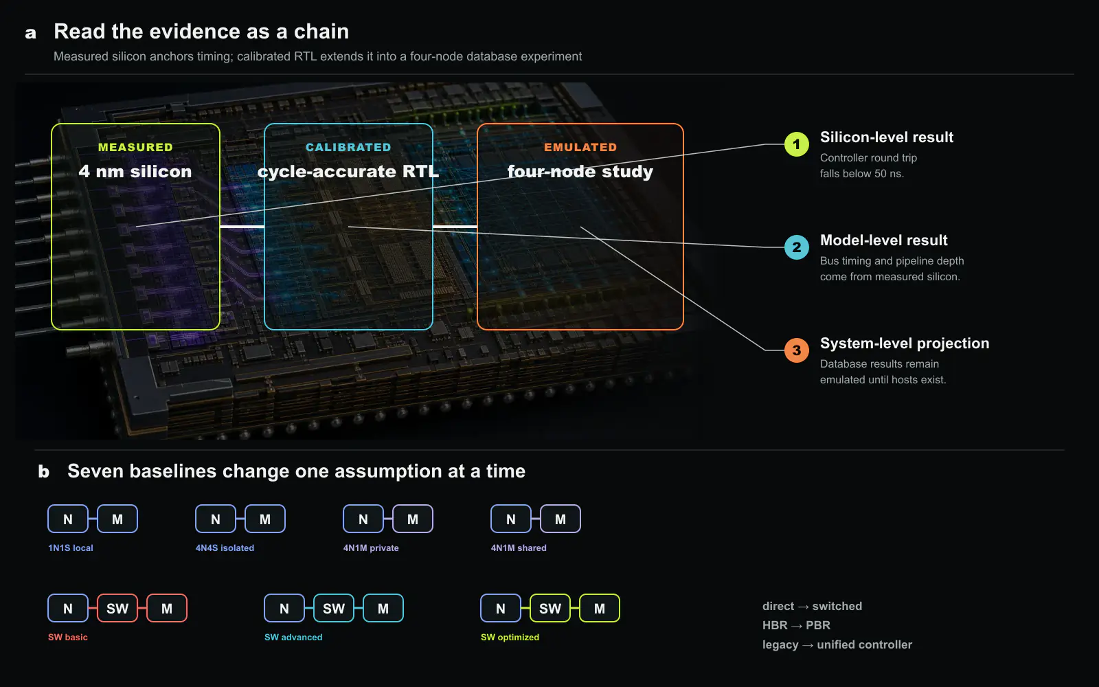
That chain matters when reading the representative numbers. Silicon measurements establish that the short controller pipeline can be built and timed. A calibrated model then asks what a system assembled from those components would do. It does not yet establish cable behavior, host interoperability, firmware maturity, or failure recovery in a production CXL 3.2 rack. The result is stronger than an uncalibrated simulation but narrower than a deployed-system measurement.
Against that setup, the headline microbenchmark follows the direction predicted by the architecture. A legacy HBR switch path costs 2.8× the round-trip latency of a direct-attached expander; swapping in the PBR switch recovers roughly 35%, and combining it with the unified controller cuts the total by 53%, a 2.1× reduction. On TPC-C, configurations with memory sharing cut storage and RDMA stalls (41% of end-to-end latency for low-hit transactions) and the full design lowers average latency by 42% versus the legacy switch. Tail behavior moves the same way: against a direct-attached baseline whose p99 runs 1.9× its p50, the proposed stack lowers p50 by 29% and p99 by 58%. Across twelve workloads, throughput reaches 4.8× the single-node baseline, versus 3.4× for the legacy switch. Node-sensitivity sweeps show near-linear scaling to 64 nodes through cascaded switches, while isolated expanders flatten at 3.7× and a private MHD actually loses 35% going from one node to four as bandwidth divides. Under a write-heavy YCSB-A, port-based scheduling holds bandwidth utilization above 95% and delivers 4× the throughput of a private MHD, and under rising concurrency the fabric absorbs 512 instances while keeping the lowest latency at both ends of the load curve. Lastly, the NUMA study shows that consolidating socket-level memory paths into the shared pool removes inter-socket hops, holding latency uniform across sockets where a single-attached device pays up to 1.7×.
Where the evidence stops
Two boundaries are worth marking. First, the division of evidence: sub-50 ns controller latency and the pipeline’s timing behavior are silicon measurements, while every end-to-end database number passed through an emulation layer, however carefully calibrated. Calibrated RTL does not guarantee the behavior of a production rack, and CPUs with PCIe 6.0 physical layers plus full CXL.cache support are required for that confirming experiment. Second, the software that showcases the fabric is not stock: PostgreSQL was modified to exploit hardware coherence for concurrent writes, which is precisely the kind of change the broader ecosystem has yet to make. The deployed CXL systems we have covered lived on the other side of both boundaries. Meta’s Vistara shipped expansion while deliberately avoiding switches, and Beluga accepted roughly 750 ns per 64 B through a CXL 2.0 switch because it still beat RDMA. This paper is aimed at the layer both of them worked around.
What we take from it
We believe the paper’s central claim survives its caveats: the roughly 2× switch overhead is an artifact of inherited silicon, not a property of CXL, and a from-scratch controller can bring a switched fabric closer to direct-attached latency. The itemized nanosecond accounting (elastic buffers, flit validation, scheduler unification) is more persuasive than one representative number because each mechanism is independently checkable. What remains unproven is everything that requires the ecosystem to move: hosts that speak CXL 3.2, software that trusts hardware coherence, and fabric management at datacenter scale. To this end, this paper reads as the component-level counterpart of the one-chip datacenter argument we covered previously[7]: that review sketched the fabric hierarchy, and this work supplies measured silicon for the switch in that hierarchy. Whether the fabric era arrives on schedule now depends less on the switch than on the CPUs that must plug into it.
Source and attribution
This article is an editorial summary prepared for Silicon & Systems. It restates the argument of the paper cited below in our own words. No text, figures or tables from the paper are reproduced here, and unless noted otherwise, the figures on this page were created for this summary; the fusion-switch photograph appears courtesy of Panmnesia. The paper was presented at ISCA 2026; the authoritative version appears in the ISCA 2026 proceedings, (c) IEEE 2026.
Disclosure: The paper is authored by Panmnesia, where the editor of Silicon & Systems serves as CEO and is a co-author of the original work. This summary should be read as coverage of our own team’s research, and the critical notes above are offered in that light.