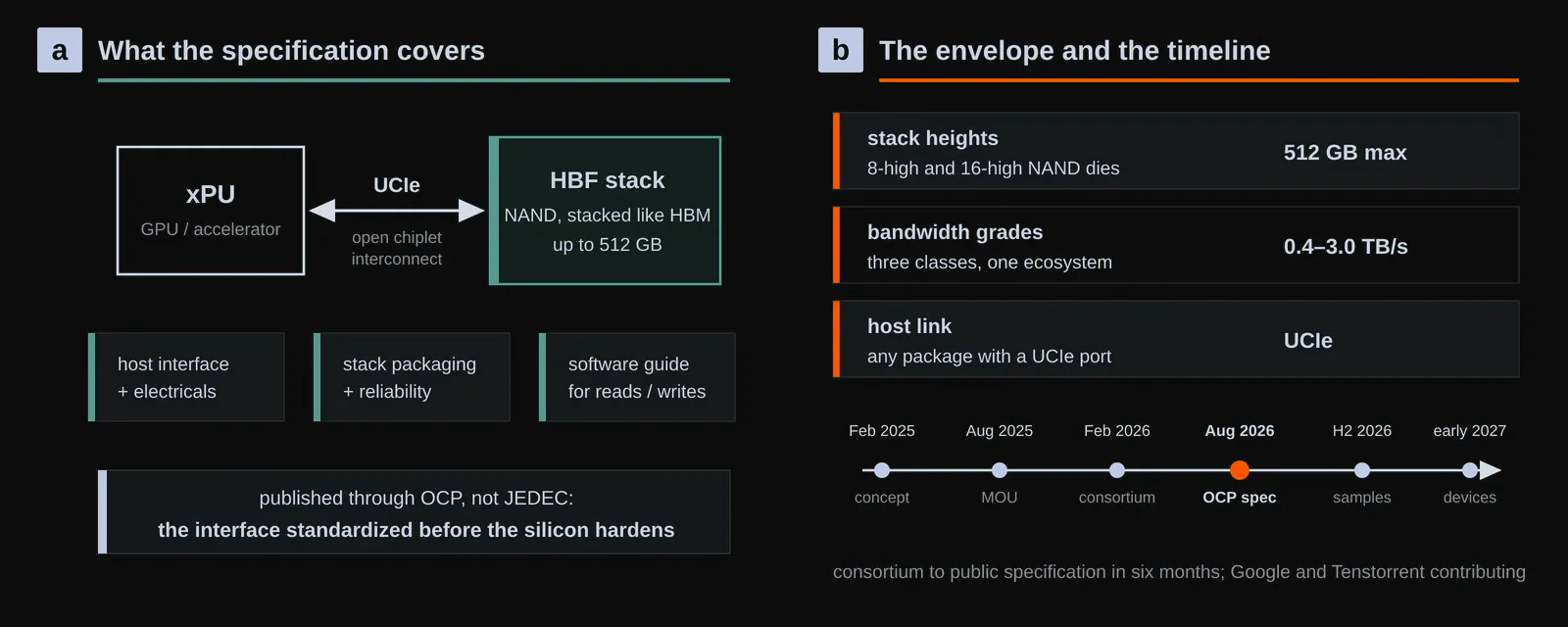
Memory technologies usually spend a decade maturing before anyone writes a standard for them. High Bandwidth Flash (HBF) went the other way. Sandisk showed the concept in February 2025, signed a memorandum with SK hynix at FMS that August, formed a standardization consortium in February 2026, and on August 3, 2026 the two companies released the first HBF technical specification through the Open Compute Project (OCP), six months after the consortium started work[1]. Google and Tenstorrent joined along the way, and Google DeepMind sat on the FMS 2026 panel that discussed where the technology fits[3]. For a memory class that did not exist two years ago, that is an unusually crowded table.
The reason for the hurry is arithmetic. Frontier model weights now occupy terabytes, while a top-end GPU carries a few hundred gigabytes of HBM, and agentic serving stacks add key-value (KV) caches that grow with every concurrent context. When capacity runs out, the industry’s standing answer has been to buy more GPUs, paying for compute in order to get the memory soldered next to it. HBF proposes a different trade: stack NAND the way HBM stacks DRAM, accept microsecond reads instead of nanosecond ones, and put half a terabyte behind each stack for the data that is read constantly but written rarely. We summarize what the specification defines, how the silicon gets there, and where the first independent measurements say the idea does and does not work.
What the specification pins down
The document is a systems contract rather than a device datasheet. It defines the xPU-to-HBF host interface, the electrical rules, packaging and reliability guidance for the die stack, baseline performance expectations, and a software guide for read and write operations[1]. Three choices matter most. First, capacity: the spec admits 8-high and 16-high NAND die stacks, reaching 512 GB per stack. For scale, a GPU that today surrounds itself with eight HBM stacks would, with the same count of HBF stacks, sit next to 4 TB. Second, speed is graded rather than fixed: three bandwidth classes span roughly 0.4 to 3.0 TB/s per stack, letting cost-sensitive and bandwidth-hungry designs share one ecosystem. Third, and most consequentially, the host link is UCIe, the open chiplet interconnect, rather than a proprietary PHY. That decision aims HBF at any package with a UCIe port (i.e., GPUs, custom accelerators, and the growing population of chiplet-based designs), not at one vendor’s roadmap.
Note that OCP is an unusual home for a memory standard; DRAM generations live at JEDEC. Publishing through OCP reads as a statement about the intended customer: hyperscalers who want to shape the interface before silicon hardens, in the body where they already standardize racks and accelerator modules.
How NAND reaches HBM territory
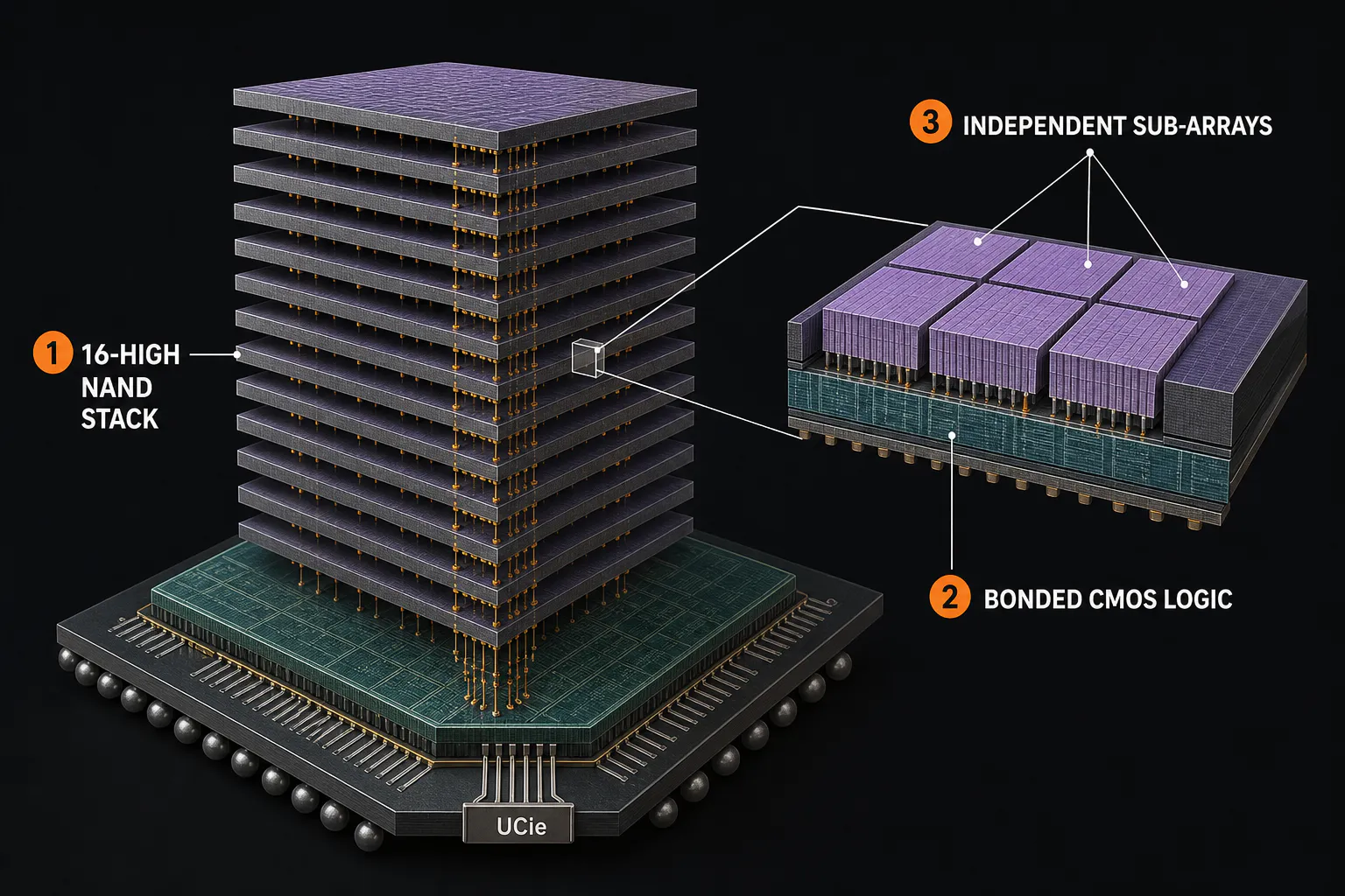
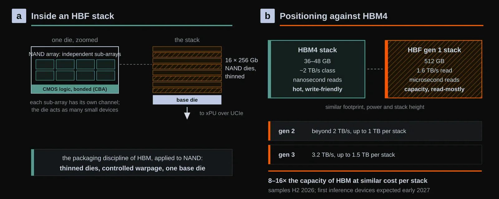
A single NAND die cannot stream anywhere near a terabyte per second, so the interesting question is how a stack of them can. Sandisk’s first-generation design answers with parallelism at two levels[2]. Within a die, the CBA (CMOS bonded to array) process bonds the logic wafer directly to the memory array and carves the array into a large number of independent sub-arrays, each with its own access channel, so a die behaves less like one slow device and more like a wide array of small ones. Across the stack, 16 dies of 256 Gb each are thinned, stacked with controlled warpage, and presented through a base die, which is the same packaging discipline HBM uses. The stated first-generation targets are 1.6 TB/s of read bandwidth and 512 GB per stack, in a footprint, power envelope and stack height close to HBM4, which is what makes drop-in-adjacent placement on an interposer plausible. Sandisk’s roadmap extends the pattern: second and third generations target beyond 2 TB/s and 3.2 TB/s, with stack capacities of 1 TB and 1.5 TB, respectively.
The economics claim is the sharpest single sentence in the announcement materials: 8 to 16× the capacity of HBM at a similar cost per stack. NAND bits are fundamentally cheaper than DRAM bits, and HBF spends that advantage on capacity rather than price. Samples are slated for the second half of 2026, with the first AI inference devices carrying HBF expected in early 2027.
The fine print is the write path
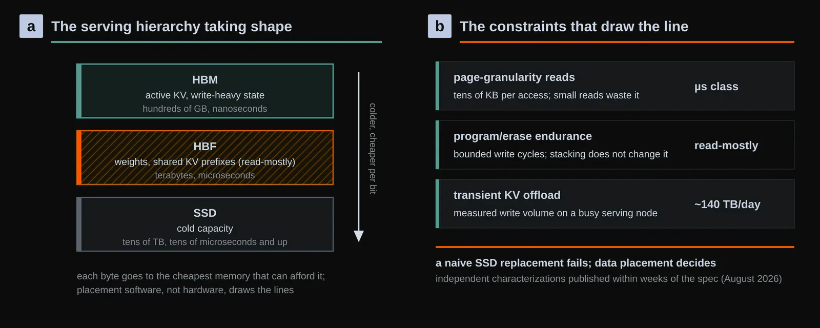
NAND did not stop being NAND. Reads complete in microseconds, roughly two orders of magnitude behind HBM, and they arrive at page granularity of tens of kilobytes, so small random accesses waste most of the bandwidth they touch. Endurance is bounded by program/erase cycles, which no amount of stacking changes. The specification acknowledges this frankly by shipping a software read/write guide with the electrical rules: HBF is a tier you must place data onto deliberately, not a transparent slab of slower HBM.
The first independent measurements, which appeared within weeks of the spec, mark the boundary precisely. A full-stack characterization aimed at KV-centric serving found that using HBF as a naive substitute for an SSD offload target fails outright: transient KV caches in a busy serving node can generate on the order of 140 TB of writes per day, a volume that collides with flash endurance while the page-granularity reads throttle effective bandwidth[4]. The same studies find the opposite result for read-mostly data. Model weights, and shared precomputed KV prefixes of the kind agentic and RAG-style serving reuse across requests, stream out of HBF at rates that keep accelerators fed[5][6]. The emerging division of labor is therefore three-layered: HBM holds active KV and write-heavy state, HBF holds large read-mostly objects, and SSDs keep the cold remainder. SK hynix has been arguing the same shape from the vendor side, proposing HBM-plus-HBF hybrid configurations for LLM inference[7], and its FMS keynote framed HBF inside a broader tiered-memory architecture for agentic AI rather than as a standalone part[3].
Readers of our earlier coverage will recognize the pattern. Meta’s Vistara worked because most of a server’s footprint is cold and a slow tier absorbs capacity rather than traffic, and Beluga rebuilt KV serving around a pooled DRAM tier precisely because KV data is read-heavy and reusable. HBF applies the same logic one level further down the hierarchy, with a thousand-fold latency gap instead of a two-fold one, which is why the placement software matters even more here.
What we take from it
A specification is not a product, and the list of things still unproven is long: no independent silicon exists yet, the 0.4 to 3.0 TB/s grades are envelopes rather than measurements, and the economics claim of similar cost per stack will be tested by exactly two suppliers, which is one fewer than the HBM market that pricing complaints made famous. However, we believe the speed and the guest list are the story. A concept went from investor-day slide to an open, multi-vendor interface specification in eighteen months, with two of the likely largest customers inside the tent before first samples, and the write-path limits documented by third parties before launch rather than discovered after. That sequence looks less like a speculative memory and more like an industry preparing a landing zone. Whether HBF becomes the fourth durable tier of the AI memory hierarchy now depends on software: the schedulers and serving stacks that must learn, as tiering software before them did, to send each byte to the cheapest memory that can afford it. The parts of that lesson learned on CXL tiers over the past three years transfer almost unchanged.
The read path and write path are different products
High parallelism can make NAND reads resemble a high-bandwidth memory tier, but writes still carry program and erase latency, endurance limits, garbage collection, and data-retention obligations. A system that markets one bandwidth number across both directions hides the mechanism most likely to disturb predictable service. Workload qualification should therefore separate sequential and random reads, sustained writes, overwrite patterns, and background maintenance.
The controller needs enough spare capacity and scheduling authority to keep maintenance from appearing as an unbounded latency spike. That may include overprovisioning, wear leveling, bad-block management, and throttling of write-intensive tenants. Each mechanism spends capacity or performance to preserve endurance and tail latency. The specification defines an interface; a product must disclose how its flash management realizes that interface over its useful life.
Persistence semantics also need labels. Completion at an on-package buffer, completion after programming NAND, and completion after protection against a power event are different guarantees. If HBF is used as a model-weight or KV tier, applications may accept reconstruction after loss. If it stores the only checkpoint copy, acknowledgment and power-loss behavior become much stricter. The same hardware can serve both roles only when software can request and observe the appropriate durability level.
Packaging creates bandwidth and concentrates risk
Stacking many NAND channels near the accelerator shortens and widens the data path. It also places flash, controller logic, interconnect, and potentially compute in one thermal and manufacturing envelope. Read-heavy inference can sustain traffic for long periods, while write and erase operations add different power behavior. Qualification should measure temperature by tier, sustained bandwidth after thermal equilibrium, error correction activity, and throttling.
Yield and serviceability affect cost. A conventional SSD can be replaced independently, while a tightly integrated package may bind the value of several components. Redundant channels, disabled dies, or capacity binning can recover partially functional assemblies, but the delivered capacity and bandwidth may vary. Buyers should know the minimum enabled configuration and whether failed capacity can be isolated without taking the accelerator offline.
Signal integrity and power delivery also scale with channel count. A package that reaches a high aggregate rate in a short benchmark must maintain it across simultaneous lanes and realistic data patterns. Error rates, retraining, and correction overhead should be included in sustained results. The valuable bandwidth is the rate delivered to the workload after protection, not the sum of raw lane symbols.
Software must decide which state belongs in flash
HBF is slower than HBM and denser than on-package DRAM, so placement policy determines its value. Model weights with predictable reuse, cold KV blocks, retrieval indexes, and checkpoints have different read size, lifetime, and urgency. A runtime should classify objects rather than expose HBF as undifferentiated capacity.
For inference, the decision can compare retrieval time with recomputation and the request’s TTFT budget. For training, it can compare checkpoint or optimizer-state movement with step and recovery deadlines. Prefetch is useful when future access is predictable, but over-prefetching can evict valuable data and consume bandwidth needed by urgent reads. Telemetry should show object class, hit value, bytes moved, queueing, and foreground-latency effect.
The memory hierarchy also needs backpressure. If writes arrive faster than NAND can sustain after garbage collection, buffering can delay the visible problem until all spare space is consumed. The runtime should receive a durable-write rate and remaining maintenance margin, not only instantaneous throughput. It can then slow producers, redirect writes, or preserve headroom for recovery traffic.
Adoption requires a workload-shaped endurance test
A buyer should replay the target mix for long enough to reach thermal and flash-management steady state. The test should include capacity near the intended fill level, background maintenance, error correction, power cycles, and a device or channel failure. Results should report read and write latency distributions, sustained useful bandwidth, write amplification, remaining endurance, and recovery behavior.
The comparison set should include HBM or DRAM capacity, conventional local SSD, and remote storage where relevant. Match usable capacity, durability, and workload outcome rather than peak interface speed. HBF may win by avoiding a remote path or by fitting more weights near compute even when its raw media remains NAND.
We read the first specification as an important standardization point, not a completed product benchmark. It defines how a denser persistent tier can enter the accelerator package and software stack. The market case will depend on controller behavior, thermal and yield evidence, object placement, endurance, and the amount of model work completed inside latency and recovery objectives over the device’s life.
Source and attribution
This article is an editorial summary prepared for Silicon & Systems. It restates, in our own words, material from the public HBF announcement and specification overview released by Sandisk and SK hynix through the Open Compute Project on August 3, 2026, together with the FMS 2026 presentations and the independent studies cited above. No text or figures from those sources are reproduced here, and the figures on this page were created for this summary. The specification and press materials are (c) Sandisk Corporation and SK hynix Inc. 2026; the cited measurement studies are (c) their respective authors.