The AI silicon genre has a house style: die shot, peak TOPS, a benchmark table, and a wave toward future work. Meta’s ISCA 2025 industry paper on MTIA 2i, the second-generation chip now serving ranking and recommendation inference to billions of users, opens by naming what that genre leaves out[1]. Architecture, the authors argue, is the smaller half of making an in-house chip pay; the larger half is co-designing models to fit the silicon, proving the chip flexible enough to survive model evolution, and absorbing everything production throws at hardware that no vendor stands behind but yourself. The headline number is a 44% average reduction in total cost of ownership against GPUs for the models launched so far, and the paper is largely an itemized account of what that number cost to earn.
We summarize the argument in our own words below.
A memory hierarchy with a hole where HBM should be
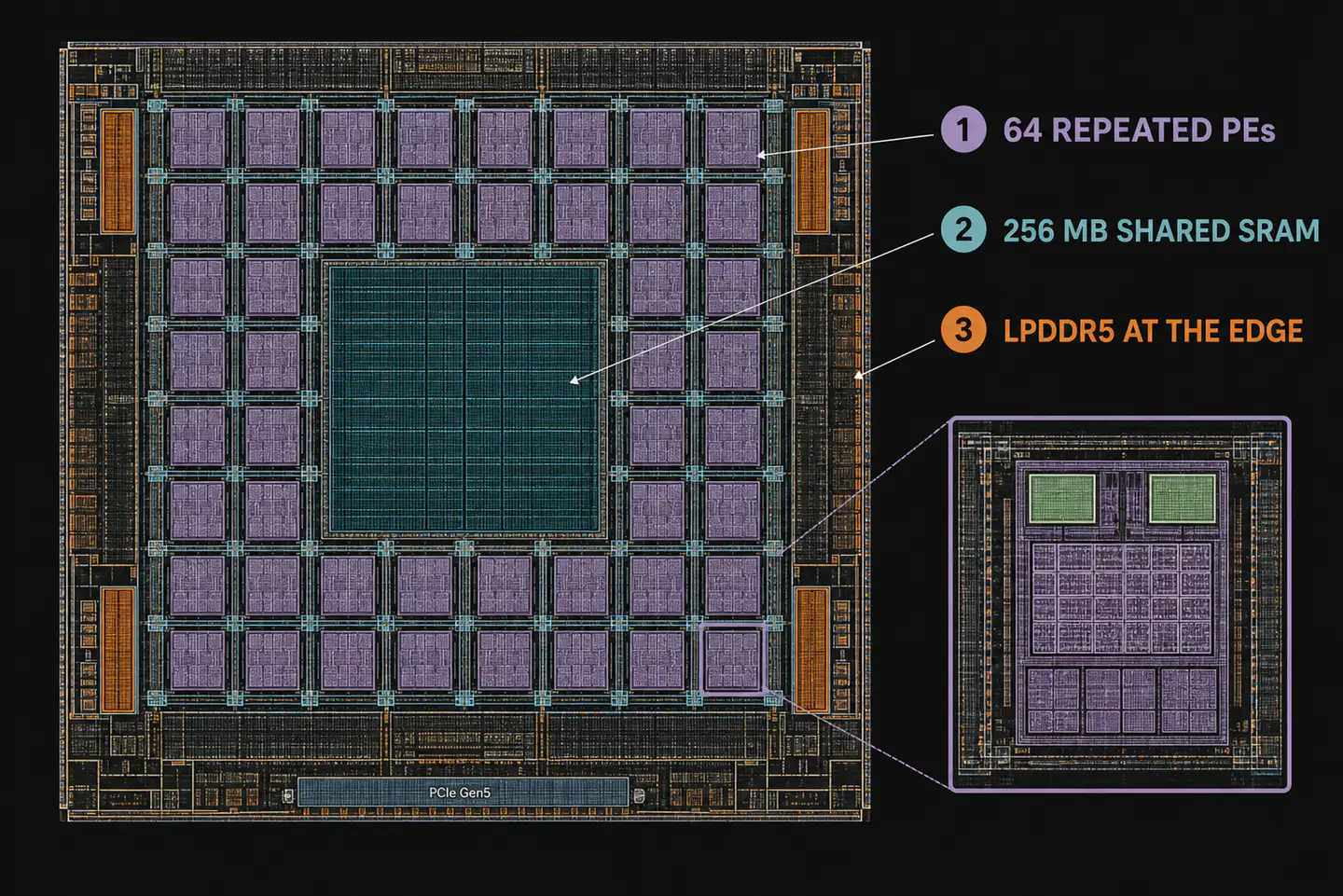
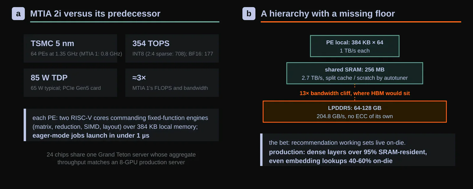
MTIA 2i is a TSMC 5 nm die of 64 processing elements at 1.35 GHz, each pairing two RISC-V cores with fixed-function engines for matrix multiply, reduction, SIMD work and layout transforms, delivering 354 INT8 TOPS (708 with structured sparsity) in an 85 W envelope, roughly 3× its 2023 predecessor[2] on compute, network-on-chip bandwidth and SRAM bandwidth. The unconventional part is what feeds it. There is no HBM: 256 MB of on-die SRAM at 2.7 TB/s sits over 64 to 128 GB of LPDDR5 at 204.8 GB/s, a 13× bandwidth cliff between tiers. The bet is that recommendation models, unlike large Transformers, have working sets with enough locality to live in SRAM: production results bear it out, with dense layers hitting over 95% SRAM residency and even the irregular embedding lookups keeping 40 to 60% of accesses on-die. Software chooses how the SRAM splits between a hardware-managed cache and software-pinned scratch, and an autotuning framework (kernel variants picked by nearest-neighbor search over a performance database, 1000× faster than exhaustive sweeps; batch sizes chosen by traffic replay) makes that choice per model, since Meta has far too many models to hand-tune. A deliberately small chip is the other half of the thesis: 24 of them share one Grand Teton server whose aggregate matches an 8-GPU box, and small units let a fleet with spiky, bursty demand allocate capacity in fine grains instead of idling monsters.
What the datasheet never tells you
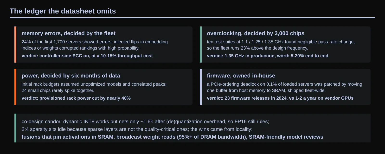
The productionization chapters are the paper’s real contribution, and each reads like a decision a vendor datasheet would have made for you. LPDDR has no native ECC, and at design time Meta genuinely did not know whether inference could shrug off bit flips, so the question went to the fleet: among the first 1,700 servers, 24% showed memory errors, and injection experiments found that flips in embedding indices or the wrong bits of a weight reliably produced NaNs or corrupted rankings. Product teams vetoed absorbing that noise, so controller-side ECC went on, at a 10 to 15% throughput penalty that every number in the paper already includes. Overclocking ran the other direction: a 3,000-chip study across ten test suites showed the silicon held margin well past its 1.1 GHz design point, and the fleet now runs at 1.35 GHz, worth 5 to 20% end-to-end. Six months of production power data let the team cut the provisioned rack budget by nearly 40%, on the observation that 24 small chips rarely peak together. And owning the firmware turned silicon errata from crises into patches: a PCIe-ordering deadlock that surfaced on 0.1% of loaded production servers was mitigated by relocating one buffer from host memory to SRAM, shipped fleet-wide through a pipeline that released 23 firmware bundles in 2024, against the one or two a year the same team manages for third-party GPUs.
Model-chip co-design gets equal candor, including about features that failed. Dynamic INT8 quantization works (row-wise activations over static INT8 weights match FP16 quality) but the quantize-dequantize overhead cuts the DPE’s 2× advantage to about 1.6× on big layers, so FP16 still rules production. The 2:4 sparsity path stays mostly idle because the layers with enough sparsity to exploit are not the layers that decide model quality. What did pay was locality engineering: operator fusions that pin activation buffers in scratch SRAM, broadcast reads that stop 64 PEs from fighting over weight traffic (over 95% of DRAM bandwidth achieved on the worst shapes), and a hard-won organizational habit of rejecting model changes that break SRAM residency and offering ML engineers an equivalent that does not. The eight-month case study tells that story end to end: one of Meta’s top-five revenue models arrived at 50% of GPU cost-efficiency, grew 6.7× in complexity while being ported, and launched at 180%.
What the numbers say
Across nine production models spanning 15 to 1,000 MFLOPS per sample, MTIA 2i lands between 0.9× and 2.1× GPU cost-efficiency, averaging the headline 44% TCO reduction, with performance per watt clustered near parity (0.8 to 1.2×), which the authors attribute to GPUs’ decades of power tuning. Efficiency tracks SRAM fit rather than complexity per se: the winners are models whose activations pin in scratch memory at large batch, and the laggards are those that spill. Validation is unusually strong for the genre, since the serving stack can split live traffic between MTIA and GPU fleets running transformations of the same trained model, and the comparison is scored on advertising revenue and prediction quality, not just latency. The boundaries are stated with the same bluntness: Llama-class LLMs do not fit (an 8 B model meets prefill targets but the LPDDR-bound decode misses its 60 ms token budget), models beyond roughly 2 GFLOPS per sample outrun the SRAM strategy, and the software ecosystem still trails the CUDA world for the long tail of small models that cannot justify manual attention.
What we take from it
Set beside the other industry silicon we have covered, this paper completes a pattern. Vistara is Meta shipping unglamorous memory expansion; MTIA 2i is Meta shipping unglamorous compute, and both papers spend their prestige on operational truth rather than peak numbers. The chip’s design thesis also reads as a mirror image of the demand-side documents: where DeepSeek’s wishlist[6] begs for more interconnect and HBM for token generation, Meta’s recommendation fleet demonstrates a large, lucrative AI workload for which the correct answer was less memory bandwidth, bought cheaper, fronted by SRAM. We believe the durable lesson is the 44% itself being an average over survivorship: MTIA 2i wins because Meta reserved the right not to run every model on it, keeping GPUs for what falls outside the design point. In-house silicon does not need to beat the general-purpose incumbent everywhere; it needs a workload census accurate enough to know where it will, and the organizational machinery (autotuning, A/B against live revenue, weekly firmware) to hold that ground as models drift. That machinery, not the PE array, is what this paper actually documents, and it is the part competitors will find hardest to copy.
The missing HBM is a workload boundary
Choosing a different memory hierarchy can improve cost for models whose weights, activations, embeddings, and intermediate state fit the intended tiers. It can also exclude workloads that depend on HBM capacity or bandwidth. The correct reading is not that HBM is unnecessary. It is that the accelerator was designed around a production portfolio with measured locality and reuse.
Every deployment should preserve that portfolio view. Group models by parameter and embedding footprint, access pattern, batchability, latency objective, and update frequency. Then map bytes and bandwidth to on-chip memory, attached DRAM, host memory, and network. A model that performs well because its hot state fits locally should not justify placement of a different model whose working set streams continuously from a slower tier.
Portfolio drift is an architectural risk. Recommendation and ranking models can grow, add features, or change sparsity faster than a chip generation. The platform needs telemetry that shows spill traffic, memory stalls, and capacity headroom by model. When those indicators cross a threshold, the operator can change placement, compress state, or move the workload rather than attributing a systemic mismatch to random performance variation.
Productionization is a repeatability claim
A custom accelerator creates value only when it can be deployed, scheduled, debugged, updated, and kept busy across a fleet. Peak kernel performance is one part of that chain. Compiler coverage, numerical agreement, host integration, observability, failure handling, and workload onboarding determine how much of the catalog can use the device without bespoke intervention.
The production report should distinguish eligible models, qualified models, and models actually running at useful scale. It should record fallback rate to CPUs or GPUs, reasons for fallback, time to qualify a new model, and performance drift across software releases. These measures reveal whether co-design lowers recurring operational cost or merely shifts it into a specialized engineering team.
Availability also needs a denominator. A fleet can have many installed accelerators but little schedulable capacity if model compatibility, host pairing, network locality, or maintenance fragments the pool. Utilization should be reported beside eligible demand and completed inference work. Otherwise, a high percentage may reflect a narrow workload while a low percentage may reflect deliberate reserve for a bursty service.
Total cost must include the paired system
The reported cost advantage belongs to a platform, not an isolated die. Host CPUs, memory, networking, storage, board power, cooling, software development, and fleet reserve all contribute to the price of a completed recommendation or ranking request. A custom accelerator can remove expensive general-purpose capability, but the surrounding system must provide whatever functions remain.
A matched comparison should run the same model, quality target, request distribution, and latency objective on the custom platform and its alternative. It should include warm and cold states, peak and low demand, model updates, and failure recovery. Energy should be measured at the server input, and cost should include usable capacity after redundancy and fragmentation.
The 44% total-cost result is therefore most valuable as evidence that Meta performed this wider accounting for a selected production scope. It should not be multiplied across every AI workload. A buyer or designer should ask which costs entered the denominator, how mature each software stack was, and whether volume and utilization assumptions remain valid for its own fleet.
Co-design should preserve a migration path
Custom silicon and models evolve on different schedules. A stable intermediate representation, compiler fallback, numerical validation suite, and compatible service interface can decouple them enough for staged adoption. New models should begin with correctness comparison, then limited traffic, then wider placement after latency, quality, and fault behavior are understood.
The platform should also support exit. If a model no longer fits the memory or operator envelope, it must move to another accelerator without changing product behavior. Keeping this path tested prevents the custom device from becoming a constraint on model progress. It also gives the scheduler an alternative during shortages or failures.
Supply and manufacturing belong in the same plan. A lower-cost accelerator that cannot be delivered in the required volume or replaced quickly can create fleet imbalance. Multiple board revisions, host dependencies, and firmware versions can fragment capacity. Production qualification should track these configurations as distinct resource types until evidence supports pooling them.
We read MTIA 2i as a systems result about specialization at portfolio scale. The architecture gives up a conventional HBM-centered design because Meta could align memory, compute, software, and workload demand. Its durable lesson is the discipline of that alignment: state the eligible portfolio, measure the complete paired system, preserve observability and fallback, and update the mapping as models and supply change.
Source and attribution
This article is an editorial summary prepared for Silicon & Systems. It restates the argument of the paper cited below in our own words. No text, figures or tables from the paper are reproduced here, and the figures on this page were created for this summary. The paper appeared in the ISCA 2025 industry track and is published under a CC BY 4.0 license; (c) 2025 the authors.