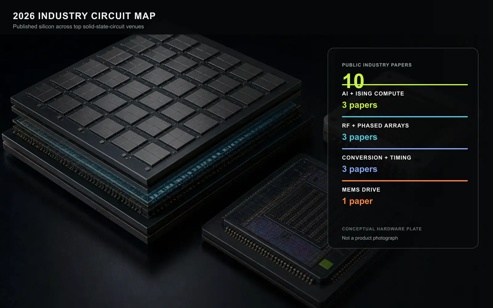
Through August 30, the 2026 public industry papers in our solid-state-circuit scope show that block-level optimization is giving way to three coupled design objects: the physical array, the control loop, and the data representation. Ten papers meet the public-full-text and company-affiliation filters. Their measured advantages depend on treating package geometry, timing correction, or structured data as part of the circuit rather than an external condition.
A time-bounded inventory
We searched ISSCC, VLSI Circuits, CICC, ESSERC Circuits, A-SSCC, and JSSC using published author affiliations and open full-text locations. The 2026 inventory is frozen at August 30, 2026. Later conference proceedings and journal assignments can add papers to the year. Therefore, “all” means all indexed works meeting the declared filters by that date, not a forecast of the completed calendar year.
All ten qualifying records were JSSC articles. This does not imply that the 2026 conferences contained no company work. It means that no additional conference paper satisfied the company, public full-text, circuit-track, and indexed-year conditions together at the cutoff.
A sampling PLL gains a robust acquisition path
XINYI’s CS-fusion PLL merges the acquisition behavior of a phase-frequency-detector and charge-pump loop with the low-noise steady-state behavior of a sampling PLL. A shared transconductance and charge-pump block interprets a pulsewidth error during acquisition and a sampled voltage after lock. The architecture keeps proportional and mixed proportional-integral paths active without the abrupt handoff used by a separate frequency-locked loop.[1]
Two silicon prototypes report a jitter figure of merit of -253.3 dB and a reference-normalized figure of merit of -248.4 dB. Enabling the fusion mechanism shortened average locking time by 4.3× relative to disabling it, or 7.3× when the comparison also removed the proportional-path assistance. Those ratios depend on the tested starting conditions. The architectural point is that acquisition and low-noise tracking can share the same phase information instead of switching between independently offset detectors.
DTC chopping attacks a fractional spur at its symmetry
Infineon and Politecnico di Milano identify even-order nonlinearity in a variable-slope digital-to-time converter as a dominant source of fractional spurs. Their loop randomly alternates the DTC location, placing it on either the reference path or the divider path. The sign change suppresses even-order error terms and also lowers the DTC flicker-noise contribution. Background digital adaptation maintains the cancellation across process, voltage, and temperature.[1]
The 28 nm synthesizer occupies 0.22 mm². Power is 16.7 mW. Measured on the near-integer channel at 9.275 GHz, its worst reported in-band fractional spur stays below -63 dBc and integrated rms jitter remains below 80 fs, producing a -249.8 dB jitter-power figure of merit. Chopping works here because the unwanted term has a predictable symmetry. It is not a generic substitute for modeling every spur path.
A 3-D Ising chip emulates a quantum model at room temperature
Ixana, Transio, Purdue, and collaborators implement a quantum Monte Carlo algorithm on a 65 nm CMOS network of probabilistic bits. A stacked logical dimension represents the Suzuki-Trotter expansion of a transverse-field Ising model, while the same reconfigurable hardware also supports conventional 2-D Ising optimization problems.[2]
For the reported quantum Monte Carlo problem at 0.5 V, the chip uses 41.9 µJ per solution when clocked at 1 MHz. Raising the clock to 10 MHz lowers that result to 16.65 µJ. The corresponding energy per elementary operation is 1350 and 535 fJ. The paper reports a three-order-of-magnitude improvement over its FPGA comparison. This is a classical emulator, not a quantum processor. Its significance is that a probabilistic circuit can make the algorithm’s local update rule the native hardware operation.
D-band user equipment becomes an antenna-in-package problem
Panasonic, Shinko Electric, Tokyo Institute of Technology, and collaborators integrate two four-element transceiver ICs into an eight-element antenna-in-package module. Its phase shifter locks by injection and triples the local-oscillator frequency while controlling phase, avoiding a long multistage D-band LO chain. A shared PA/LNA path and subharmonic mixer reduce duplicated RF hardware.[3]
The module operates from 142 to 164 GHz, reaches 25.7 dBm EIRP, and demonstrates 56 Gb/s. Each element consumes 150 mW in transmit and 93 mW in receive from 1 V; the 65 nm transceiver occupies 8.5 mm². The 0.088 mm² LO phase-shifting block itself consumes 15 mW. At these frequencies, the module is the circuit: antenna loss, package transitions, LO distribution, and thermal density determine whether the IC result remains useful.
A 300 GHz transmitter removes the combiner
NTT and university collaborators place the power amplifier last in each of four phased-array paths. An optimized transistor layout raises the reported gain-corner frequency, while a dual-peak maximum-gain core broadens interstage matching. Each element drives an on-chip Vivaldi antenna, so no output power combiner sits between the PA and radiation.[4]
The PA maintains more than 20 dB gain from 237 to 267 GHz. The array sends 60 Gb/s 16-QAM over 6 cm and 56 Gb/s QPSK over 20 cm, with 16.2 dBm peak EIRP at 245 GHz. A stacked-board 4 × 4 measurement scans ±24° in one plane and ±28° in the other. These are short-range laboratory links, but they establish that removing a lossy combiner and co-designing the antenna can preserve useful modulation at 300 GHz.
Energy recovery changes the MEMS-driver voltage budget
Infineon and Technical University of Munich use a bipolar series-parallel switched-capacitor charge pump to drive an ultrasonic capacitive load. Conventional hard charging discards the reactive energy proportional to frequency, capacitance, and voltage squared. The proposed sequence reconfigures flying capacitors to step the load through positive and negative voltages and recover part of that energy.[5]
The integrated driver produces 1.8 to 41.1 Vpp waveforms at 450 kHz and reports a power-reduction factor as high as 16.3. Compared with its unipolar counterpart, the bipolar arrangement nearly doubles both peak-to-peak voltage and the reduction factor while needing about half as many stages for a given swing. Parasitic capacitance limits the ideal gain, which is why the measured integrated result is more informative than the lossless charge-pump equation.
A 256-element satellite transmitter calibrates polarization locally
Axelspace and collaborators build a 19 GHz, 256-element active array for low-Earth-orbit terminals. A 90° coupler-end structure generates circular polarization with less active overhead and can emit two opposite polarizations in different directions. Two calibration procedures correct cross-polarization error in single- and dual-polarization modes.[6]
At 56 dBm average EIRP, the array consumes 9.4 W, which the paper reports as 40% below its state-of-the-art comparison. Maximum EIRP is 64.7 dBm at 17.8 W. Beam steering reaches ±65° with sidelobes below -10 dBc. The measured link supports 256-APSK at 2 Gbaud in single-polarization mode and 250 MBaud per path in dual-polarization mode at the stated 56 dBm EIRP. The result ties polarization generation, calibration, and array power to one terminal-level operating point.
A delta-sigma feedback DAC avoids linearity calibration
Infineon and University of Ulm use a sturdy multistage-noise-shaping digital modulator to drive the feedback DAC of an 80 MHz continuous-time delta-sigma converter. The shaped multi-DAC arrangement reduces sensitivity to element mismatch. An intersymbol-interference shuffler and gain-boosted DAC cells address dynamic memory effects that would otherwise limit wideband linearity.[7]
Across an 80 MHz band, the 28 nm prototype measures 106.2 dB SFDR without DAC linearity calibration. Its 2.75 GHz clock and reported figure of merit of 163.7 dB show the cost of maintaining that range. The relevant claim is narrower and stronger than “calibration free”: the feedback-DAC linearity does not require a foreground or background coefficient calibration under the reported measurements.
Few-shot learning keeps training on the edge
TSMC and UC San Diego extend the hyperdimensional-learning line into FSL-HDnn, which integrates a weight-clustered feature extractor with a gradient-free few-shot classifier. Early exit can stop feature extraction at an intermediate branch, while batched single-pass training raises utilization when several labeled examples arrive together.[8]
The 40 nm chip reports 6 mJ per image and 28 images/s for a 10-way, five-shot training task, with 2.9 TOPS/W for the stated operation. End-to-end training is 2× to 20.9× faster than the paper’s comparison set while maintaining the reported task accuracy. The important boundary is that feature extraction and class update share one measured datapath; the energy number is not extrapolated from a classifier core alone.
Structured bit sparsity preserves regular hardware
NXP, imec-linked university researchers, and collaborators organize nonzero weight bits into bit columns before execution. SparseCol exploits this training-free structured bit-level sparsity while a dynamic dataflow maps different neural-network shapes onto the available lanes. The design tries to keep memory access and compute regular without an expensive online scheduler.[9]
Fabricated in 16 nm, the chip reaches 1320 BTOPS/W peak, where BTOPS counts binary operations as weight bits multiplied by activation bits and conventional operations. CNN and transformer system evaluations report 745.02 and 850.5 BTOPS/W. The authors report a 6.8× efficiency gain over their sparse-processor comparison. Because BTOPS depends on precision accounting, readers should compare the definition as carefully as the value. The architectural contribution is the conversion of irregular zeros into a structure the memory and datapath can consume consistently.
Structure moves from an optimization to the specification
Several 2026 papers cannot state their contribution without the surrounding structure. The D-band transceiver is an antenna-in-package module, the 300 GHz transmitter ends in on-chip radiators, and the 256-element satellite design combines polarization and calibration with the array. IC, package, antenna, and beam policy form one measured object.[3][4][6]
The compute papers make the same move in data representation. The Ising chip maps a probabilistic update into native p-bit behavior, FSL-HDnn stores learned classes as hypervectors, and SparseCol arranges nonzero bits into regular columns. Efficiency arises because the data is redefined before it reaches the arithmetic, not because a conventional datapath simply runs faster.[2][8][9]
Timing and conversion papers structure the error. CS-fusion combines acquisition and sampling behavior, DTC chopping uses error symmetry, the delta-sigma design shapes DAC mismatch, and the MEMS driver recovers charge through a controlled switching sequence. In each, a result depends on the state machine or symmetry surrounding the nominal block.[1][5][7]
Three disclosure tests for a headline number
First, identify the physical hierarchy. Is the measurement a core, chip, package, module, array, or link? EIRP from an antenna-integrated array cannot be compared with PA output power, and driver efficiency depends on the actual capacitive load. The boundary must travel with the number.
Second, identify the control state. PLL acquisition and locked tracking are different regimes; a calibrated array and an uncalibrated one are different systems; energy recovery depends on switching sequence and parasitics. A best steady-state point should not imply that startup or transition is free.
Third, identify the operation definition. Binary operations, conventional MACs, probabilistic updates, feature extraction, and classification produce incompatible TOPS denominators. Absolute task latency, energy, quality, and silicon conditions are necessary before cross-paper comparison.
What the 2026 evidence still leaves open
The RF demonstrations establish impressive frequency, modulation, beam, and integration points, but field range, blockage, thermal density, calibration aging, and manufacturing variation remain product questions. The Ising result is classical hardware executing a quantum Monte Carlo formulation, not a quantum processor or a proof of advantage on every optimization problem.
The learning chips demonstrate measured on-device training or sparse inference under selected tasks. They still need broader distributions, model evolution, security of updates, and software-toolchain evidence. The MEMS driver and delta-sigma converter need load and variation coverage beyond the reported points.
These limits do not weaken the annual pattern. They identify where the co-designed structure must next survive: package, field environment, application distribution, or lifecycle calibration. That next boundary is the proper subject of product validation.
The 2026 design pattern
The ten results make one boundary increasingly difficult to ignore: a circuit block cannot be evaluated apart from the structure that feeds and surrounds it. The D-band transceiver is inseparable from its package and antenna. The MEMS driver is defined by the capacitive load and recovered charge. The PLLs depend on error symmetry and acquisition state. The learning accelerators depend on how bits or classes are represented before they enter the array.
For system evaluation, every headline efficiency should therefore be paired with three questions. What physical hierarchy was measured? Which control state produced the result? Which operation definition counts the work? A 2026 design that answers all three is more informative than a larger number from an isolated core.
Source and copyright notice
This article is an independent editorial synthesis of the ten cited papers, covering records available through August 30, 2026. Technical ideas and measurements are restated in original language; no IEEE figure or table is reproduced. The package-scale hardware plate was generated specifically for this article and labeled deterministically. It is not a product image or manufacturing drawing. The cited works are © IEEE 2026, with two articles carrying 2025 DOI registration dates. Public access to an author manuscript is not treated as permission to reuse the publisher presentation.