The unit of competition in AI infrastructure has quietly moved from the chip to the rack. Whoever defines how a few hundred accelerators inside that rack read each other’s memory collects a growing share of the bill: by one estimate in the UALink Consortium’s own commissioned analysis, $15 to 25 M of a $100 M deployment now goes to interconnects[2]. NVIDIA holds the incumbent position with NVLink, and since October 2024 an unusually broad coalition (a board drawing AMD, Intel and Synopsys from silicon, Alibaba, AWS, Google, Meta and Microsoft from the cloud, plus Apple, Astera Labs, Cisco and HPE, with over 115 members in total) has been building the open challenger, UALink. The consortium published its 200G 1.0 specification in April 2025 with a white paper by AMD’s Nathan Kalyanasundharam[1], and followed in January 2026 with a longer third-party analysis that, unusually for consortium literature, names its rivals and argues against them line by line[2]. This article reads both documents closely, and places them against the Ethernet counteroffensive and the one scale-up fabric already running at supernode scale in production, Huawei’s Unified Bus.
What UALink 1.0 actually defines
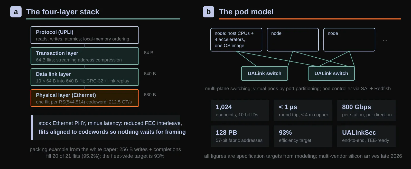
Strip the advocacy and the specification makes concrete, checkable commitments. UALink is a memory-semantic fabric: accelerators issue reads, writes and atomics of 64 to 256 bytes against a 57-bit fabric address space (128 PB), under the same ordering model that applies to an accelerator’s local memory, so a pod of up to 1,024 endpoints programs like one very large device rather than a network[1][2]. Each endpoint carries a 10-bit routing identifier; switches route by destination, and a pod can be carved into isolated virtual pods by partitioning switch ports. The stack is four thin layers. A protocol interface (UPLI) hands 64-byte flits to a transaction layer that compresses addresses with a streaming cache; the data link layer packs ten of those into a 640-byte flit protected by CRC-32 with link-level replay; the physical layer aligns each such flit to one RS(544,514) forward-error-correction codeword and ships it over standard IEEE 802.3 signaling at 212.5 GT/s per lane (200 GT/s of data), with a latency-reducing reduction of FEC interleaving as one of the few deviations from stock Ethernet[1].
The design targets follow from those choices: four lanes form an 800 Gbps-per-direction station, request-to-response round trips stay under 1 µs over copper runs below 4 meters spanning one to four racks, and protocol efficiency reaches 93% of physical bandwidth, illustrated in the white paper by 256-byte writes with completions riding 20 useful flits out of 21[1][2]. Two less-advertised inclusions deserve notice. UALinkSec specifies end-to-end encryption and authentication of all protocol channels, designed to hold even against a physically present adversary and to slot into confidential-computing TEEs, which reads like a hyperscaler procurement checkbox written into silicon. Manageability, likewise, is delegated to existing datacenter machinery (a pod controller driving switches through SAI, nodes through Redfish) rather than a new proprietary stack.
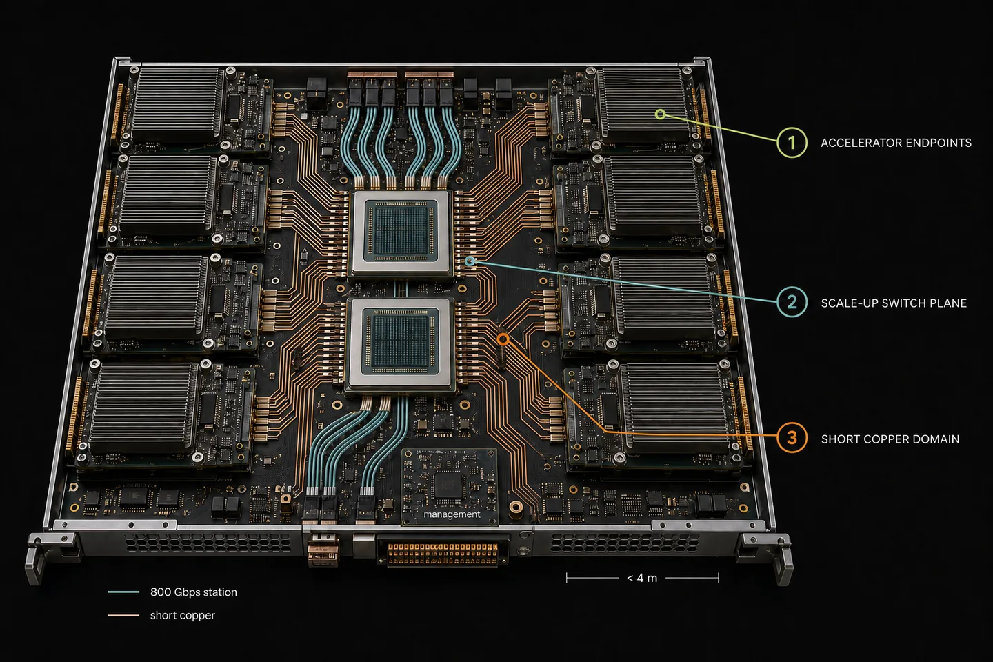
Equally instructive is what the documents decline to define. Inter-pod communication is explicitly out of scope. Ring and torus topologies are permitted but deadlock avoidance on them is the implementer’s problem. The software ecosystem above the fabric (collective libraries, the NCCL equivalent) belongs to members, not to the specification. In addition, every performance number in circulation is a target validated by modeling and protocol simulation: the January 2026 analysis states plainly that empirical multi-vendor verification is planned for 2026, with evaluation switch silicon expected late in the year[2]. UALink today is a completed paper standard awaiting its first hardware referendum.
The incumbent and the two counterattacks
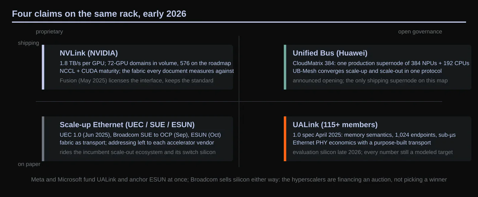
NVLink remains the benchmark the documents measure against: 1.8 TB/s per GPU in its fifth generation, NVSwitch domains of 72 GPUs shipping in volume with configurations to 576 on the roadmap, and a decade of NCCL and CUDA maturity that no specification can conjure[2]. NVIDIA’s most telling move came in May 2025 with NVLink Fusion, which licenses selected partners to implement NVLink-compatible interfaces. The consortium’s analysis is quick to note that Fusion opens the interface without opening the standard (NVIDIA keeps certification, evolution and per-partner terms), but the concession itself acknowledges that a closed fabric had become a procurement liability at nine-figure deployment sizes.
The second counterattack came from Ethernet, and it arrived in a single crowded year: the Ultra Ethernet Consortium’s 1.0 specification in June 2025 with credit-based flow control and link-layer retry, Broadcom’s Scale-Up Ethernet framework contributed to OCP in September, and ESUN, an OCP initiative to standardize Ethernet scale-up networking, in October[4][5][6]. The UALink analysis meets this camp with two architectural distinctions rather than a dismissal. First, addressing: the Ethernet side leaves the fabric as transport, with address translation belonging to each accelerator vendor (SUE says so outright), while UALink defines one fabric-level address space every compliant device shares[2][4]. Second, flow control: Ethernet’s CBFC runs one credit loop per link, while UALink stacks independent credit domains at every boundary (six in a single-hop path), buying finer backpressure at the cost of more protocol state. Note the sociology underneath: Meta and Microsoft sit on UALink’s board while anchoring ESUN, and Broadcom can sell merchant silicon into either ecosystem.
Standing apart from both is the one system already operating at the scale everyone else is specifying toward. Huawei’s CloudMatrix 384 connects 384 Ascend NPUs and 192 CPUs into a single supernode over its Unified Bus, and the UB-Mesh work extends the ambition to datacenter scale with a converged scale-up/scale-out protocol that Huawei has said it will open[8]. Whatever one makes of its ecosystem, it is the only entry on this map with production supernodes rather than projections.
August 2026 update: both open camps filled a gap
Two releases after this article’s original January publication change the comparison, although neither constitutes deployed silicon. UALink Common 2.0 now introduces in-network compute, while separating the common protocol from speed-specific data-link and physical-layer documents[3]. This matters because a switch can reduce, combine or otherwise transform collective traffic while it is already in flight, rather than forwarding every partial result to an accelerator. The specification page states the intended benefits as lower latency, lower bandwidth consumption and better scaling for distributed training and inference. It answers the largest functional omission we identified in UALink 1.0, but the answer remains a specification until implementations and collective libraries expose measured behavior.
ESUN also moved from initiative to document. OCP released its Network Operator Requirements Base Specification 1.0 on March 10, 2026, four months after launch[5]. It calls for lossless Ethernet through Priority Flow Control or Credit-Based Flow Control, link-level retry, and a compact four-byte ESUN header in place of the much larger IP/UDP stack for small messages. The document has a different job from UALink’s memory-semantic protocol: it states what an operator needs from an Ethernet scale-up network, not a shared accelerator address model. Thus, “open versus proprietary” is too coarse a comparison. The live design choice is now memory semantics plus an open fabric, or a lean Ethernet transport that preserves more vendor freedom above it.
The demand side has already published its order
What makes this standards race legible is that the customers have written down what they want, in venues we have covered. DeepSeek’s ISCA paper prices the scale-up domain in tokens per second (a 67 token/s decode ceiling on 400G NICs against roughly 1,200 inside an NVL72-class domain) and asks for memory semantics with hardware ordering, acquire/release in place of fences, and one converged domain instead of an NVLink-InfiniBand seam[7]. The same wishlist demands in-network broadcast and reduction for MoE dispatch and combine. UALink 1.0 left that work above the fabric; Common 2.0 now brings it into the standard, which is a meaningful response even though measurements are still pending[3]. From the opposite flank, the InfiniteHBD argument shows a fabric needs no switch at all if ring all-reduce is the only traffic that matters, at 31% of NVL-72’s interconnect cost[9]. That result reminds us that any-to-any generality is valuable only when the workload uses it. Beneath both sits CXL: the January analysis positions UALink between the node-local tier (PCIe, CXL) and the scale-out network, and its 128 PB address space anticipates disaggregated and CXL-expanded memory[2]. The one-chip datacenter argument and UALink are therefore adjacent layers rather than rivals.
What we take from it
The paper race is no longer about whether either open camp can publish a credible stack. Both can. The next evidence must come from hardware and operations. We would watch three things: measured multi-vendor efficiency against UALink’s 93% modeled target; collective-library support that makes Common 2.0 in-network compute usable without vendor-specific detours; and the first production purchase orders for non-NVLink scale-up domains. ESUN adds a fourth test: whether its four-byte header, lossless behavior and multi-hop congestion controls remain simple when different accelerators supply the address and coherence machinery above them. NVLink’s moat in 2026 is still shipping systems plus NCCL, not merely SerDes. The open side has now answered more of the architecture checklist, but specifications do not reveal yield, interoperability, software maturity or total cost. Those four measurements, rather than the membership list, will decide the rack.
A specification is not yet a deployable domain
Publishing link, transaction, and management behavior is necessary, but a rack product also needs interoperable controllers, switches, cables, retimers, endpoint logic, firmware, telemetry, and a repair procedure. The first deployment question is therefore which combinations have been tested together and at what scale. A standards logo or member list cannot substitute for a multi-vendor conformance matrix.
Operators should ask for three layers of evidence. The electrical layer must sustain the declared reach and error rate through the intended cable and connector budget. The protocol layer must demonstrate discovery, ordering, flow control, retry, and fault isolation under congestion. The system layer must run the target collective and memory-access mix while a link or endpoint fails. Passing only the first layer proves a link, not an operational scale-up domain.
This distinction also changes schedule risk. Silicon availability, switch software, cable qualification, and collective-library support may mature at different times. A cluster plan should name the minimum interoperable configuration that can ship, then identify which later features expand topology, availability, or performance. Treating the full roadmap as available on day one turns a standards comparison into a procurement assumption.
Openness should be measured at the replacement boundary
An open specification creates value when an operator can replace one component without replacing the entire domain. That boundary may sit at the cable, switch, endpoint controller, management API, or collective library. Each boundary requires compatible behavior and enough telemetry to diagnose a mixed-vendor failure. If only one complete stack can pass qualification, the protocol is open on paper but the deployed system remains vertically integrated.
The opposite extreme also has a cost. Too many optional behaviors can produce combinations that conform individually but perform unpredictably together. Profiles and implementation agreements are therefore not a retreat from openness. They define the subset that buyers can test. The useful question is whether those profiles are controlled by one vendor, a broad consortium, or a customer-led qualification process.
Comparisons with NVLink and Ethernet should use this replacement test. NVLink offers a mature integrated path with less component choice. Ethernet offers a broad supply chain but may require more software and congestion engineering for scale-up semantics. UALink aims to occupy the middle. Its success depends on whether independent endpoints and switches can meet one workload and failure contract, not only whether their packets share a format.
Deployment should preserve an escape path
The first rack should not make the rest of the fleet dependent on an unproven domain. A practical design contains failure within the rack, exposes standard scale-out networking above it, and lets the scheduler place jobs on either the new or established platform. This permits matched comparisons and keeps a firmware or supply problem from blocking all training capacity.
The acceptance report should state delivered collective bandwidth, message-size sensitivity, tail latency, performance under one failed link, recovery time, power per delivered bandwidth, and the software versions used. It should also identify workloads that do not benefit, such as jobs too small to use the domain or communication patterns that map poorly to the topology. A technology becomes credible when its non-target region is as clear as its peak.
We read UALink as a contest over who can define the rack’s replacement boundaries. The protocol can diversify supply only if conformance, management, and collective software make those boundaries real. Until multi-vendor systems demonstrate that outcome, the specification establishes direction and negotiating leverage, while product evidence must still establish capacity.
Sources and disclosure
This article is an original analysis by Silicon & Systems, based on the public documents cited below, principally the UALink 1.0 and Common 2.0 materials, the January 2026 commissioned analysis, and OCP’s ESUN 1.0 release. No text, table or figure from those documents is reproduced; the figures on this page were created for this article. Disclosure: the editor of this site is CEO of Panmnesia, a company building CXL fabric silicon discussed in adjacent coverage. This article touches CXL only peripherally, but that interest may influence our framing.