Every scale-up domain shipping today assumes a switch. NVIDIA’s NVL-72 wires 72 GPUs through trays of NVLink switch silicon, Google’s TPUv4 routes between 64-chip cubes through centralized optical circuit switches, and the open standards racing to catch up (UALink, scale-up Ethernet) are, at bottom, specifications for what such a switch should speak. A SIGCOMM 2025 paper from StepFun, the LLM lab, with the silicon photonics vendor Lightelligence and Peking University, asks what happens if the switch simply goes away[1]. Their answer, InfiniteHBD, moves circuit switching into the transceiver itself: every 800 Gbps optical module carries a small Mach-Zehnder interferometer matrix that can steer light between two external paths and an internal loopback. Out of nothing but these modules, the design builds rings of any size across a datacenter, isolates faults to single nodes, and prices its interconnect at 31% of NVL-72 per GPU per GB/s. The price of admission is architectural honesty: the fabric does rings, and only rings.
We summarize the argument in our own words below, and flag where the evidence is measured hardware and where it is simulation.
The case for a bigger, stretchier domain
The paper opens with a workload study that doubles as the design’s justification. Using an in-house training simulator on Llama 3.1-405B, the authors find that the tensor parallelism (TP) size that maximizes Model FLOPs Utilization grows with cluster scale, from 16 at 1,024 GPUs to 64 at 65,536, while a fleet locked to TP-8 (the size an 8-GPU server imposes) falls behind by up to 3.37× at 131,072 GPUs. Since TP synchronizes with ring all-reduce, whose traffic touches only logical neighbors, a domain that supports large TP does not actually need any-to-any bandwidth; it needs long, reliable rings. For Mixture of Experts models the authors go further and argue TP can substitute for expert parallelism (EP): EP moves less data in theory, but real routers hand experts unequal token counts, and once that imbalance passes roughly 10% the straggler effect erases EP’s communication advantage in their simulations of a 1.1 T-parameter model. In their sweeps the optimal EP degree comes out at 1.
Note that this worldview is contested territory. DeepSeek’s ISCA paper, which we covered previously, treats large-scale EP all-to-all as the defining traffic of MoE inference and asks for fabrics that accelerate it[5]. InfiniteHBD bets the opposite way for training: shard experts evenly under TP, keep the traffic neighborly, and build the cheapest possible fabric for exactly that pattern. Which bet ages better depends on whether MoE serving or MoE training sets the fabric requirements, and the two papers make instructive opposite reads of the same tension.
Three architectures, three failure geometries
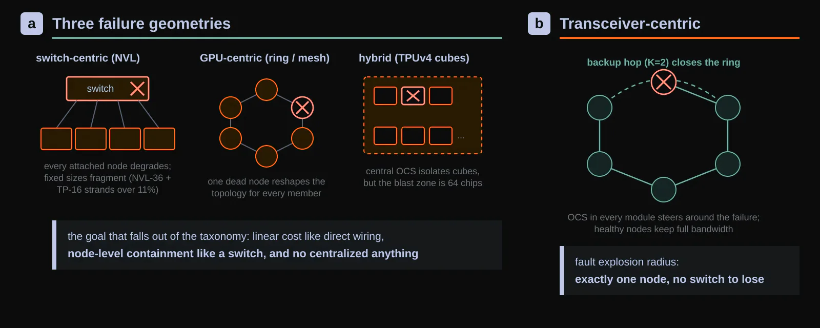
The taxonomy section is the paper’s sharpest analytical tool. Switch-centric domains (NVL-36/72/576) buy any-to-any communication with switch chips whose cost grows superlinearly with scale, and a failed switch degrades every attached node. Their fixed sizes also fragment: a domain of 36 GPUs running TP-16 strands at least 11% of its capacity, since 36 minus a failure is not divisible by 16. GPU-centric designs (TPUv3, Tesla’s Dojo, the SiP-ML ring proposal[3]) delete the switch and wire accelerators to each other, which scales linearly in cost but couples fates: one dead GPU reshapes the topology for everyone, a property the authors call an HBD-level fault explosion radius. TPUv4 splits the difference with optical switches between 64-chip cubes[2], which contains failures, but only to a 64-chip blast zone, and the centralized OCS hardware carries its own cost and manufacturing burden. The design goal falls out of the taxonomy: linear cost like GPU-centric designs, node-level failure containment like switch-centric ones, and no centralized anything.
A circuit switch that fits in a QSFP-DD shell
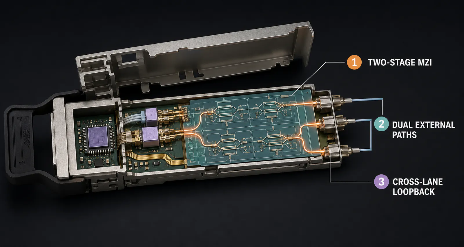
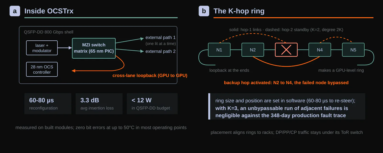
The enabling hardware is the part of the paper that exists as measured silicon. OCSTrx integrates a silicon photonic OCS into a standard QSFP-DD 800 Gbps transceiver: a 65 nm photonic chip of 10.5×13 mm carrying the MZI switch matrix, driven by a 4×4 mm 28 nm controller. Two MZI stages make the initial routing decision (external path 1, external path 2, or loopback), and an internal crossbar handles lane-level loopback between the module’s two attached GPUs. Thermo-optic phase arms reconfigure the light path in 60 to 80 µs, orders of magnitude faster than the milliseconds-to-minutes of MEMS, piezo or robotic optical switches, and fast enough to hide behind a training step. The measured penalties are small: 3.3 dB average insertion loss at room temperature (2.5 to 4.0 dB across parts), zero bit errors at up to 50°C in most operating points, and under 12 W total module power, within the QSFP-DD envelope. Because switching happens per-transceiver, only one external path is lit at a time, so the full GPU bandwidth follows whichever connection is active instead of being split across standby links.
The topology assembled from these modules is a K-hop ring: each node runs optical links to its neighbors at distance 1 through K (K=2 or 3 in practice), giving every node 2K escape routes. In healthy operation a TP group forms a GPU-granular ring by activating loopback at the two ends of a chain of nodes, so ring size is set by software, at any position, in any length. When a node dies, its neighbors reconfigure to the backup hop that reaches past it, and the ring closes again with the radius of the failure held at exactly one node; with K=3 the probability of an unbypassable run of adjacent failures becomes negligible against their fault statistics. A placement algorithm then co-orchestrates the ring domain with the ordinary datacenter network, aligning TP groups to racks so that the parallelism dimensions that do cross the Ethernet fabric (data, pipeline, context) stay under their top-of-rack switches.
What the numbers say, and which machine they ran on
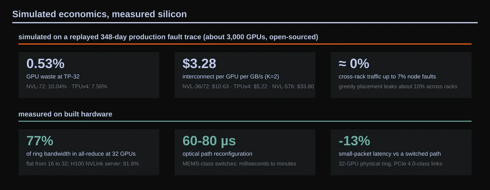
The evaluation splits cleanly into a hardware layer and a simulation layer. The transceiver numbers above are bench measurements of built modules, validated over PCIe and Ethernet lane rates and through temperature cycling. A 32-GPU cluster wired as a physical ring (experimental GPUs with PCIe 4.0-based inter-host links) measured all-reduce at 77.1% of ring bandwidth for 16 GPUs and 77.3% for 32, against 81.8% for an H100 NVLink server, with 13% lower small-packet latency than the switched path; the encouraging part is the flat curve from 16 to 32, since rings are supposed to get worse as they grow.
Everything else is simulation, though unusually well-grounded simulation: the fault model replays a 348-day trace from StepFun’s production cluster of roughly 3,000 GPUs, which the team has open-sourced. Under that trace, running TP-32 jobs, InfiniteHBD strands 0.53% of GPUs, against 10.04% for NVL-72 and 7.56% for TPUv4 (19× and 14× better, respectively), and the K=2 configuration tracks K=3 closely enough that the third hop looks optional at production fault rates. On cost, the paper’s bill-of-materials analysis puts the interconnect at $3.28 per GPU per GB/s for K=2, versus $10.63 for NVL-36/72 (30.9%) and $5.22 for TPUv4 (62.8%), with NVL-576’s multilayer fabric reaching $33.80. The orchestration algorithm holds cross-rack traffic near zero up to a 7% node fault ratio where a greedy placement leaks about 10% of traffic across racks. The headline 3.37× MFU gain, however, should be read as the value of unlocking TP-64 at 131,072 simulated GPUs rather than as a measured speedup, and it leans on a simplification the authors disclose: their large-TP simulations replace Llama’s grouped-query attention with classic multi-head attention, which inflates how much TP a real 405 B model would want.
Where the evidence stops
Three boundaries deserve marking. First, no training run at scale has crossed this fabric: the largest physical artifact is a 32-GPU ring on PCIe 4.0-class links, and every fleet-level claim (waste ratios, cost, MFU) passes through the in-house simulator, however carefully calibrated against production traces. Second, the architecture’s candor about all-to-all cuts both ways. A ring executes EP-style traffic in O(p²) exchanges; the authors sketch a binary-exchange variant that would close the gap for small groups, then decline to build it because of the failover and orchestration complexity it drags in. If MoE inference economics push fabrics toward all-to-all, as DeepSeek argues, a ring-only domain serves the training half of the fleet, not the whole. Third, multi-dimensional parallelism inside one domain (TP and EP at once, say) requires either dedicating transceiver bundles per dimension or time-dividing the optics, both of which erode the clean story. The comparison set also deserves one asterisk: the NVL-72 cost figures are assembled from public and secondary sources, which the authors acknowledge, and vendor pricing at hyperscale rarely resembles list.
What we take from it
The scale-up argument has mostly been a contest between bigger switches: NVLink domains today, UALink and scale-up Ethernet tomorrow, and, on the coherent-memory side, the CXL fabrics we have covered in one-chip datacenter design and Panmnesia’s switch silicon. This paper stakes out a genuinely third position: for the one traffic pattern that dominates large-model training, the cheapest switch is none, and reconfigurable point-to-point optics can deliver domain sizes no switch fabric will reach at comparable cost. We believe the paper’s most durable contribution is not the particular ring topology. It is the demonstration that OCS can live inside a commodity transceiver with microsecond-class reconfiguration, a capability that Google needed room-sized switches to obtain[2][4]. Specifically, once the light path itself becomes software-defined at the endpoint, topologies can follow workloads rather than the other way around. Whether the industry backs any-to-any switching or rings, the transceiver demonstrated here can serve either direction.
The control plane must prove the topology it requested
Moving switching into the transceiver distributes the data plane, but it also makes topology state a safety concern. Before a collective begins, every endpoint must agree on which optical paths are active, which node has been bypassed, and which ring ordering the communication library will use. A stale route can partition the collective or direct traffic into a loop. The controller therefore needs a versioned topology transaction with confirmation from the modules before exposing the new communicator to the job.
Reconfiguration time is only one term in that transaction. Fault detection, path calculation, module programming, optical settling, link training, communicator repair, and collective replay determine the interruption visible to training. The measured 60 to 80 µs switch time demonstrates fast hardware, but a deployment should report the complete recovery interval and the amount of lost work under node and link failures.
This requirement also defines the comparison with packet switches. A conventional fabric pays more per port but offers mature routing, telemetry, isolation, and repair. Endpoint OCS must reproduce the subset required by synchronous training at lower total cost. If it can, the absence of a central switch is a system advantage. If orchestration needs extensive spare links and conservative barriers, part of the optical saving returns as control-plane capacity.
Source and attribution
This article is an editorial summary prepared for Silicon & Systems. It restates the argument of the paper cited below in our own words. No text, figures or tables from the paper are reproduced here, and the figures on this page were created for this summary. The paper appeared at SIGCOMM 2025; the authoritative version is in the Proceedings of the ACM SIGCOMM 2025 Conference, (c) 2025 the authors, publication rights licensed to ACM. An author-prepared version is openly available at arXiv:2502.03885.