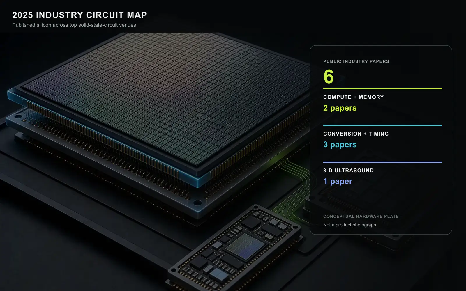
The 2025 public industry record is smaller than the 2024 set under the same filters, but its design direction is unusually consistent. Six papers place precision control inside the operation that creates the error. They do not wait for a large backend to repair reference ringing, PCM conductance error, sampling distortion, cable count, oscillator injection weakness, or retraining cost.
Scope and completeness
The inventory uses the same venue boundary as the 2024 review: ISSCC, VLSI Circuits, CICC, ESSERC Circuits, A-SSCC, and JSSC. We require a company affiliation in the published author record and an openly reachable full-text location. Official program tracks were checked for VLSI and ESSERC. Six works satisfied all conditions for 2025. The count describes this reproducible public subset, not the full volume of company-authored circuit research.
An asynchronous SAR pipeline fixes latency and reference behavior together
Analog Devices and KU Leuven split a low-noise SAR ADC into two stages and allow their decisions to progress asynchronously. The purpose is not merely throughput. The second stage adds precision without tying conversion latency to the external sample period. Reference snubbers at the clock-domain crossings damp settling and ringing for the sub-ADCs and floating-inverter residue amplifier.[1]
The 40 nm prototype reports 71.1 dB peak SNDR and 77 dB dynamic range at 200 MS/s while consuming 5.8 mW. Conversion latency remains 8 ns under the stated operating method, and the reported Schreier figure of merit is 179.4 dB. The result shows that reference distribution is part of converter architecture. A faster comparator cannot recover precision if the reference network is still moving when the next decision begins.
PCM programming approaches an analog weight
STMicroelectronics and Italian university collaborators treat a phase-change-memory cell as a continuously adjustable conductance rather than a small set of coarse states. Their programming algorithm iteratively approaches a target and validates the result on a 28 nm FD-SOI analog in-memory-compute prototype that performs 512 × 512 signed matrix-vector multiplications.[2]
The reported programmed-weight equivalent number of bits is 10.55. That number characterizes programming precision under the experiment, not the end-to-end accuracy of every neural network or the long-term stability of all conductance levels. Drift, temperature, array-scale distributions, and repeated-update cost remain system conditions. Still, a converter-quality metric above ten bits changes what can be assigned to the memory array and what must remain in digital compensation.
The sampling front end reaches Ka band without a mixer
The University of Twente and Teledyne built a four-way time-interleaved front end at 12.8 GS/s with 38 GHz tracking bandwidth. An inductor-assisted input network, push-pull buffers, and active bootstrapping extend the first track-and-hold. A single first-rank sampler avoids the skew and bandwidth-mismatch calibration that multiple parallel front samplers would require.[3]
Four measured samples maintained more than 39 dB SNDR through a 32 GHz input while the front end consumed 87 mW. The authors estimate about 25 fs of total aperture jitter, and the input return loss remains better than 12 dB through 35 GHz. This is enough to directly subsample the targeted 27-31 GHz satellite band. The architectural gain is the removed RF mixer, but the clock-jitter and input-network requirements move directly onto the ADC front end.
A 4096-element probe makes channel reduction a package function
The Philips collaboration expands its earlier 2048-element ultrasound chip into a probe containing two ASICs and a 4096-element CMUT array measuring 23 × 23 mm². Each ASIC serves 2048 elements. A 2 × 2 delay-and-sum micro-beamformer followed by 2× time-division multiplexing reduces receive channels by 8×, while an on-chip pseudorandom training sequence enables equalization that lowers TDM crosstalk by 10 dB.[4]
In the reported setup, the probe reaches 2000 volumes/s while covering 60° in both angular dimensions and 10 cm in depth. Receive and logic power are 0.85 and 0.10 mW per element, while nominal transmit power is 0.34 mW per element and depends on the waveform. The important progression from the 2024 conference chip is not only twice the element count. It is the demonstration that array, two ASICs, cable reduction, equalization, and transmit programmability can operate as one probe.
A PLL injects on both halves of the reference cycle
University College Dublin and MediaTek alternate two charge-sharing capacitors so that positive and negative reference half-cycles both reinforce the LC tank. This ping-pong path implicitly doubles the injection opportunity. A frequency-tracking loop and duty-cycle calibration keep the scheme operating across process, voltage, and temperature, while a low-power bang-bang detector supervises the adjustments.[5]
In 28 nm CMOS, the roughly 27 GHz PLL reports 42 fs rms jitter at 14 mW. The injection strength is three times that of the comparison charge-sharing structure, and the reference spur improves by about 15 dB. The reported jitter-normalized figure of merit is -276.6 dB. The mechanism matters more than the record value: both halves of a reference period become useful energy-transfer events, provided calibration keeps their timing and duty cycle aligned.
Continual learning replaces backpropagation with a searchable representation
The UC San Diego and TSMC Clo-HDnn accelerator targets learning after deployment. It combines a weight-clustered feature extractor with hyperdimensional computing, which stores learned classes as hypervectors rather than repeatedly updating a deep network by gradient descent. A Kronecker-product encoder compresses the representation cost, and progressive search stops after enough of the query hypervector has been compared.[6]
The chip reports 4.66 TFLOPS/W for feature extraction and 3.78 TOPS/W for classification. Progressive search reduces the evaluated work by as much as 61% under the reported tasks. Those efficiencies use different operation definitions and should not be collapsed into one number. The system result is that continual learning can be made predictable when the expensive feature extractor is reused and the update itself becomes a compact, gradient-free class representation.
The papers close six different control loops
The ADC shapes error around its reference crossing and resolves asynchronously, so the next stage does not wait for a global worst-case conversion interval. The PCM macro reads cell conductance and adjusts programming rather than assuming one pulse produces one analog value. Both designs spend local feedback to reduce static margin.[1][2]
The Ka-band sampler and ultrasound probe move system partition boundaries. Direct subsampling removes an RF mixer but transfers stringent jitter and input-network demands to the converter. Micro-beamforming and time-division multiplexing remove receive channels before the probe cable, then add equalization to control the new crosstalk path.[3][4]
The PLL uses both reference half-cycles as injection opportunities and relies on calibration to preserve their symmetry. The continual-learning accelerator turns an update into hypervector operations rather than backpropagating through a deep network. One reuses a previously idle timing event; the other changes the representation so an expensive algorithm is no longer needed on device.[5][6]
This view links papers that cannot share a performance score. Each identifies a costly open-loop assumption, introduces a local state or structure, and reports whether silicon kept the correction stable.
Local correction has a hidden observability requirement
A feedback mechanism is useful only when its controlled variable can be measured cheaply and early enough. The PCM macro needs a conductance read whose cost does not erase programming gains. The PLL needs frequency and duty-cycle information that tracks process, voltage, and temperature. The ultrasound link needs training data that identifies TDM crosstalk. The learning accelerator needs a distance measure that predicts the correct class before progressive search stops.
Readers should therefore ask what sensor, estimator, or training sequence closes each loop. Its resolution, latency, stability, and energy belong in the result. A paper can reduce the headline block while moving cost into an unreported calibration engine. The strongest works include that control path in measured power and area or state its external requirements.
Local loops also interact. A converter’s timing change can affect reference behavior; a sampler’s clock correction can alter input bandwidth; a probe’s equalization depends on package and cable. System validation should vary temperature, supply, load, and aging together rather than proving each coefficient once at room conditions.
Integration changes what “measured” means
The six works span a circuit block, memory macro, sampling front end, packaged probe, PLL, and learning accelerator. A die measurement can establish transistor and local-loop behavior. A packaged measurement adds bond, antenna, cable, or load parasitics. An application demonstration adds data, software, and accuracy. These evidence levels should not be collapsed.
The 4096-element probe provides the widest system integration in the set because array, two ASICs, multiplexing, equalization, and imaging geometry operate together. The Ka-band front end proves high-frequency sampling but leaves the downstream converter and complete receiver as system choices. The PCM macro validates programming control while array-scale endurance and application accuracy remain further steps.
This is not a ranking of paper quality. It identifies the next risk. Buyers and designers should request evidence at the boundary where a claimed saving could be lost: package, clock, memory array, cable, or software workload.
Precision and efficiency denominators remain local
The papers report SNDR, energy per conversion, programming precision, tracking bandwidth, jitter, per-element power, and TOPS/W. None can be averaged. Even similar labels can differ: the feature extractor and classifier in the learning chip use different operation definitions, while the sampling front end reports analog quality rather than completed digital conversions.
A fair reading retains absolute values and conditions. For the ADC, keep bandwidth, resolution, and reference behavior. For PCM, keep target conductance distribution, pulses, readback, and endurance. For the sampler and PLL, keep input or carrier frequency, jitter, and power. For ultrasound, keep array geometry, volume rate, depth, angular coverage, and per-element budgets. For learning, keep task, accuracy, training examples, and which stages the energy includes.
This discipline makes cross-paper synthesis possible without manufacturing a false leaderboard. The common conclusion comes from mechanism and boundary, not one normalized number.
What still needs system-level evidence
The asynchronous ADC must show how its reference and timing behavior scale in a complete converter and over variation. PCM control needs array-level yield, drift, endurance, and workload accuracy. Direct Ka-band sampling needs the rest of the receive chain and clock generation. The probe needs sustained thermal, cable, and image-quality validation in its intended use.
The injection PLL’s calibration must remain stable across startup and field conditions. Continual learning needs protection against distribution shift, class growth, and errors accumulated by the fixed feature extractor. These are the points where a local correction can become an operational maintenance burden.
The annual review therefore treats silicon measurement as the beginning of deployment evidence, not its conclusion. A result becomes more transferable when it states which variable the circuit controls and which variables remain outside the loop.
A practical reading checklist
For every circuit, locate the expensive baseline action, the new local mechanism, the state it observes, the measurement boundary, and the condition that breaks the improvement. Then ask whether the controlled state can be calibrated and monitored after fabrication. This checklist applies equally to an ADC transition, memory cell, high-frequency sampler, probe channel, PLL phase, or learned class representation.
It also clarifies process choice. A mature node may be selected for voltage handling, analog devices, or cost; a denser node may support memory and digital learning. Process alone does not explain the measured gain. The architecture is credible when the mechanism survives the physical environment for which that process was chosen.
The checklist should end with a deployment denominator. Estimate how often the controlled event occurs, how much energy or latency the correction saves each time, and what calibration, area, or software it adds continuously. A mechanism that wins a rare corner may be less valuable than a smaller gain on every conversion, memory write, or inference.
Lifecycle evidence is the final gap. Local feedback can compensate fabrication variation, but aging and environment can move the target beyond its calibration range. Products need telemetry that indicates when correction margin is exhausted and a safe fallback that does not silently degrade accuracy. These requirements connect a one-time silicon measurement to years of operation.
Reading the six papers this way turns them from isolated records into design choices: remove a boundary only when the new local loop can be observed, bounded, and maintained.
The 2025 design pattern
All six works reduce the distance between an error and its correction. The ADC damps its reference crossing, PCM programming closes the loop on conductance, the Ka-band sampler removes an external frequency-conversion step, the probe reduces channels before its cable, the PLL reuses the otherwise idle reference half-cycle, and the learner updates hypervectors instead of a full model.
This suggests a practical evaluation rule. Ask not only how much precision or efficiency a chip reports, but also where its control loop terminates. A result is more likely to survive system integration when the variable being corrected remains local, observable, and bounded by the same hardware that created it.
Source and copyright notice
This article independently synthesizes the six cited papers. It restates their technical ideas and measured results in original language and does not reproduce publisher figures or tables. The conceptual hardware plate was generated for this article and labeled with code; it is not a photograph or layout of any reported device. The cited works are © IEEE 2025. Public manuscript access is not treated as a license to reuse the IEEE presentation.