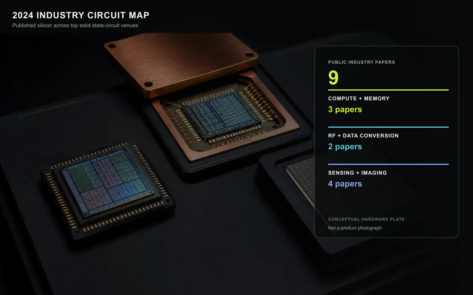
The most useful company paper is not the one with the largest headline number. It is the one that exposes a constraint, changes the circuit structure, and then measures whether the change survived silicon. Across the 2024 public record, nine papers met that standard within our scope. Their common move was to replace an expensive correction step with structure placed closer to the signal or data.
What “all” means in this review
We searched ISSCC, the Circuits track of the Symposium on VLSI Technology and Circuits, CICC, the Circuits track of ESSERC, A-SSCC, and JSSC. A paper entered the inventory when its published author metadata included a company affiliation and an openly reachable full-text location. The search covers works assigned to 2024 by the bibliographic record. Device-only VLSI and ESSERC tracks were excluded after checking the official program. Public access is an availability condition, not permission to reuse publisher figures.
This method found nine circuit papers. It does not claim that only nine industrial papers existed. It says that nine satisfied the venue, circuit-track, company-affiliation, year, and public-full-text filters together. The distinction matters because company-heavy conferences contain many papers whose manuscripts remain behind publisher access controls.
Security becomes part of the compute datapath
The IBM and MIT digital in-memory-compute macro treats physical leakage as a datapath problem rather than a wrapper added after design. Its bit-serial multiply uses linear XNOR operations on shared values, while a carry-save tree keeps shares separated without demanding thousands of new random bits every cycle. An on-chip ASCON engine decrypts model weights, and an SRAM-derived physical unclonable function generates the secret key without exposing it off chip.[1]
The 14 nm macro reached 8.1 TOPS/W at 0.50 V. The authors tested the protected compute beyond one million traces under their targeted side-channel experiments. This is evidence for the implemented attack setup, not a universal security proof. The engineering implication is nevertheless concrete: security can preserve in-memory-compute density when the arithmetic representation, accumulation tree, key path, and memory cell are co-designed.
Beamforming moves into the converter loop
NXP and Eindhoven University of Technology inserted passive R-2R vector modulators into the feed-in path of a continuous-time delta-sigma ADC. The converter therefore performs spatial weighting before a blocker consumes the internal dynamic range. The four-element prototype suppresses as many as three equal-power spatial interferers by more than 30 dB, covers 200 MHz of bandwidth, and reports more than 70 dB of spatial-blocker dynamic range at 7.3 mW.[2]
This architecture changes the partition between RF beamforming and conversion. It is attractive when an array must reject a strong direction before quantization, but the result does not remove array calibration, antenna mismatch, or front-end linearity constraints. It shows that the ADC loop itself can become a spatial filter, thereby reducing the burden placed on every downstream bit.
A phase-transition device implements neuron dynamics
IBM Research Europe and collaborators used nanoscale vanadium-dioxide devices to build the nonlinear element of a FitzHugh-Nagumo neuron. A self-coupling branch produces mixed-mode oscillations that are difficult to express with a simple phase-only oscillator. The paper compares coupled FitzHugh-Nagumo and Kuramoto-style relaxation oscillators in simulation and uses measured device behavior to support the circuit model.[3]
The contribution is a device-and-circuit demonstration, not a trained application accelerator. Its value is that the richer neuron dynamics emerge from the phase transition and coupling topology rather than from a long digital state machine. Scaling to a useful network still depends on device spread, coupling programmability, readout, and learning rules. The correct conclusion is therefore that VO2 expands the available oscillator dynamics, not that it has already displaced digital neuromorphic hardware.
Radar waveforms stop waiting for a fractional-N PLL
NXP’s ISSCC transmitter synthesizes the automotive radar waveform directly with a 7-bit I/Q DAC whose double-balanced mixer runs at 14 GS/s across 76 to 81 GHz. Digital generation removes the chirp-settling bottleneck of a swept fractional-N synthesizer and also supports coded waveforms. Under the reported filtering condition, the 1 GHz chirp showed 0.0052% relative rms frequency error. The corresponding values fell to 0.0033% at 2 GHz and 0.0016% at 4 GHz, while settling remained within 1.56 ns.[4]
The same chip demonstrated up to 102.4 Gb/s with single-carrier QAM, showing that the hardware is a wideband waveform engine rather than a one-purpose ramp generator. The price is visible in clocking and power: the LO chain consumed 79.2 mW, the mixing DAC 42 mW, and the maximum-rate baseband circuitry 54 mW. Direct digital synthesis wins when waveform agility and near-instant settling justify that budget.
Auxiliary sensors attack energy and area first
TDK InvenSense and the University of Pavia built a BJT temperature sensor around an error-feedback, noise-shaping SAR conversion process. Current-mode signal processing removes an op amp, while feedback pushes SAR quantization error out of band. In 180 nm CMOS, the sensor occupies 0.057 mm², draws 34 µA from 1.8 V, and resolves 92 mK in 80 µs across a measured -50 °C to 110 °C range.[5]
Those numbers fit the actual role of a temperature sensor inside a motion-sensing system. It does not need the finest possible resolution at any cost. It must be small, cheap to calibrate, and inexpensive enough in energy that compensating another sensor remains worthwhile. The paper is a reminder that an auxiliary circuit should be optimized against the uncertainty of the system it corrects.
High voltage can lower an accelerometer’s analog power
The University of Michigan, Nvidia, and InvenSense took the opposite-looking route for a triaxial MEMS accelerometer: generate a larger bias voltage so the mechanical signal rises above the analog front-end noise. This removes the need for a power-intensive low-noise amplifier and chopping. Fine control of the differential bias also cancels electrostatic mismatch after fabrication.[6]
Input-referred noise in the two-chip prototype measures 121 µg/√Hz, with a ±1.5 g range. Linearity error stays below 1%. Each axis uses 184 nW including high-voltage generation. Its reported figure of merit improves by 10.3× over the comparison set. The general lesson is not that high voltage is free. It is that energy spent on the transducer bias can save more energy than suppressing noise after a weak signal has already entered the electronics.
A neural implant radio removes the crystal
Tsinghua University and Beijing Ningju Technology combined differential 16-pulse-position modulation, pulsewidth modulation, and differential binary phase shift keying in an all-digital IR-UWB transmitter. A bi-phase ring oscillator built from 42 stages supplies the required timing edges, avoiding an external crystal while maintaining a sixth-order modulation space.[7]
The transmitter delivered 1.8 Gb/s at 4.09 mW, or 2.3 pJ/bit. An ex vivo setup reported transmission across 18 mm of pork tissue over a 20 cm path. These conditions do not establish an implanted clinical link, but they do address two concrete integration pressures: multi-gigabit raw neural data and the volume cost of a precision crystal.
RRAM reliability becomes an adaptive write policy
Weebit Nano and CEA-Leti evaluated read-before-write, current limiting, write termination, verification, and error correction on a 128 kb RRAM macro in 130 nm CMOS. None of those assists is new in isolation. The contribution is their coordination through a smart-write algorithm that selects the work needed by each cell and operation.[8]
The reported combination reduced write energy by 83% and access time by 55%. After one million cycles, the measured read margin was 28.1 µA with no observed read error in the stated experiment, corresponding to a reported bit-error rate below 10^-7. Adaptive control is doing two jobs here: avoiding unnecessary pulses and containing device variability. That makes the controller part of the memory technology, not merely its interface.
The ultrasound probe reduces channels before the cable
Philips and Dutch university and medical-center collaborators monolithically integrated a 2048-element capacitive micromachined ultrasonic transducer array with interface electronics. Arbitrary-wave transmit beamforming, 2 × 2 receive micro-beamforming, and 2× time-division multiplexing reduce the receive channel count by 8×. The 11.7 × 23.4 mm² array produced 3-D imaging at 2000 volumes/s in the reported setup.[9]
The decisive boundary is the probe cable. Thousands of raw channels cannot simply be exported without adding conductors, power, and mechanical burden. Local delay-and-sum processing trades some flexibility for an eightfold reduction before data leaves the probe. The 2025 JSSC extension doubles the element count and packages the same architectural idea into a fuller probe, which we treat in the next annual review rather than counting it twice here.
Three ways the papers move a system boundary
The nine papers can be read through where they place an operation that previously sat elsewhere. The secure IMC macro moves protection into the arithmetic and key path. The beamforming ADC performs spatial rejection before quantization consumes dynamic range. The ultrasound chip reduces receive channels inside the probe before signals reach the cable. In each case, the claimed efficiency comes from preventing expensive data or interference from crossing a boundary.[1][2][9]
A second group turns correction into a local feedback decision. The temperature sensor shapes conversion error, the RRAM macro adjusts writes from observed cell behavior, and the accelerometer compensates mismatch around a high-voltage transducer. These designs do not eliminate variation. They sense a bounded variable close to its source and spend correction only where it changes the output.[5][6][8]
The remaining works use physical dynamics or direct synthesis to remove an intermediate abstraction. VO2 devices provide nonlinear oscillator behavior, the radar transmitter generates wideband waveforms without waiting for a swept PLL, and the neural radio avoids a crystal reference. Their evidence is strongest when the removed block’s cost is measured together with the new timing, calibration, or device constraint.[3][4][7]
How to compare results across such different circuits
Headline efficiency cannot be ranked across a security macro, ADC, transmitter, memory, and imager. Their operations, process nodes, voltage domains, and included boundaries differ. The common comparison is causal: identify the original system cost, the circuit mechanism that moves or removes it, the silicon measurement, and the condition under which the cost returns.
For security, ask which attack model and trace count were tested. For converters and sensors, retain bandwidth, resolution, range, and calibration. For radios, keep carrier, modulation, distance, and reference assumptions. For memories, include endurance distribution and verify cost. For imaging, count array elements, channel reduction, depth, field of view, and power per element. A record without these denominators is a specification, not system evidence.
This method also prevents process-node comparison from dominating. A mature-node sensor can be the better design when area, leakage, voltage handling, and integration matter. A leading-node compute macro can be valuable because it places security in a dense datapath. The technology choice should be evaluated against the physical function rather than used as an automatic ranking.
What remained unproven in 2024
Several papers demonstrate a block or prototype rather than a complete deployed product. Side-channel traces do not certify every attack, device simulations do not establish a trained neuromorphic system, and a laboratory radar or neural link does not include the entire field environment. The annual record should preserve these boundaries instead of turning measured silicon into a market forecast.
Integration creates the next evidence request. Does calibration remain stable over temperature and aging? Does channel reduction preserve image quality in a full probe? Does an adaptive write policy maintain throughput over endurance? Can the secured compute path be provisioned and updated without exposing keys? These questions connect an impressive block to the system that must operate it.
The strongest 2024 lesson is therefore not that one circuit class won. It is that measured silicon is most informative when it makes an old cost locally observable and controllable, then reports the new limitation honestly. That standard remains useful after the headline record is surpassed. It preserves the engineering reason behind the measurement. That context matters.
The 2024 design pattern
These papers cover unrelated products, yet their most durable idea is shared. The protected IMC macro changes its arithmetic representation; the beamforming ADC rejects a direction inside the loop; the radar chip synthesizes the waveform instead of steering a slow PLL; the sensors spend energy at the transducer or quantizer boundary; the RRAM macro adapts each write; and the ultrasound ASIC reduces channels before the cable.
For a designer, the practical test is therefore where the correction happens. If a system waits until after conversion, communication, or memory access, it pays to repair a larger stream. The 2024 industrial record shows multiple cases where moving the decision one boundary earlier produced the measured advantage.
Source and copyright notice
This article is an independent editorial synthesis of the nine papers cited above. Titles, authors, measured results, and technical ideas are summarized in new language; no publisher figure or table is reproduced. The hardware landscape was generated specifically for this article and labeled deterministically. It is a conceptual package-and-die scene, not a photograph of any reported chip. The cited proceedings and journal articles are © IEEE 2024 (with some manuscript records carrying an earlier DOI registration year). Open manuscript availability does not by itself grant permission to reuse the publisher layout or figures.