HBM obtains bandwidth by making the interface wide. That physical choice creates a less visible problem inside the memory die: many data groups need accurate sampling clocks at the same time. A conventional clock-distribution network generates four quarter-rate phases, I, Q, IB, and QB, near the incoming write data strobe and then drives all four across long metal routes. At 2.5 GHz, each phase has a 400 ps period. Every repeater and routed capacitance switches billions of times per second, whether the destination is close or far.[1]
The ISSCC 2025 paper by Jeongbeom Seo, Yoonseo Cho, Yuhwan Shin, and Jaehyouk Choi changes where those four phases are created. It sends one lower-frequency signal that carries the phase sequence across the die, then reconstructs four quadrature clocks beside each DQ group with an injection-locked quadrature-clock generator (IL-QCG). The local generator consumes 850 µW in the reported 2.5 GHz operating point and covers 2 to 5 GHz. More importantly for HBM, it can stop when the write strobe disappears and resume with a useful phase from the first returning edge.[1][2]
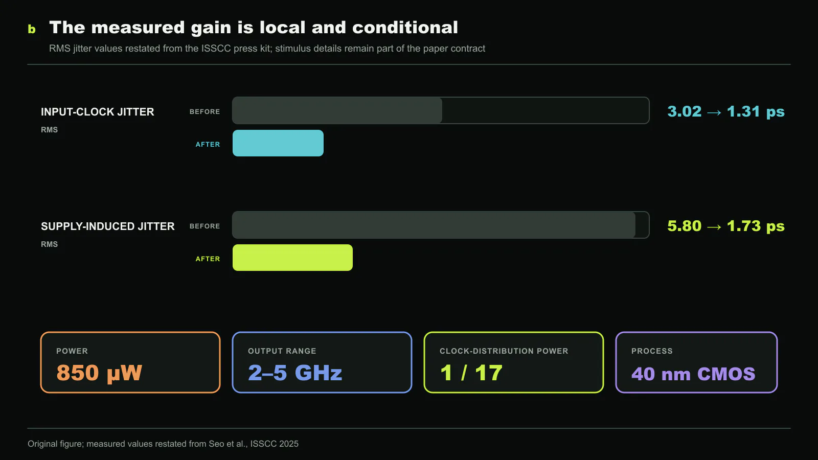
This is not a claim that an HBM stack consumes 850 µW or that total HBM power falls by a fixed percentage. The prototype measures a clock-generation and distribution method in 40 nm CMOS. Its strongest evidence concerns the clock path: a proposed 17-fold distribution-power reduction, input-jitter filtering from 3.02 to 1.31 ps RMS, and supply-induced jitter reduction from 5.80 to 1.73 ps RMS under the paper’s test conditions.[1][2] The system question is whether this local regeneration remains correct after the full die, package, voltage, temperature, activity, and manufacturing distributions are included.
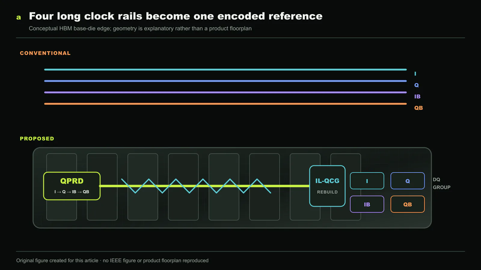
Why four phases become a routing problem
Quarter-rate operation trades clock frequency for phase count. A data path that transfers multiple bits per full-rate cycle can sample with four edges spaced by 90 degrees, allowing the internal clock to run at a lower frequency than the external data rate. The four clocks must still arrive with the intended spacing. A phase error moves one sampling edge toward the data transition and subtracts directly from timing margin.
HBM makes this difficult for three reasons. First, the interface has many DQ pins and several DQ groups within each data word. The paper describes an HBM4-oriented organization with 64 DWORDs, 32 DQ pins per DWORD, and six DQ groups per DWORD.[1] The exact commercial floorplan can differ, but the scaling direction is clear: more destinations multiply clock loads.
Second, the routes are constrained by area. Four matched wires, their shields, and repeaters compete with data, power, test, and control wiring. Narrow metal increases resistance, while unequal loading creates quadrature error. A correction block at the destination can repair phase spacing, but it does not recover the energy already spent toggling four long networks.
Third, the local power grid is not quiet. Large groups of data drivers and receivers change current rapidly around commands. Supply movement changes repeater delay, so a clean source clock can acquire power-supply-induced jitter (PSIJ) while crossing the die. A destination-only delay-locked correction loop can align phases yet still pass much of that timing noise.
The design target is therefore not merely a clock buffer with lower power. It is a distribution contract that simultaneously reduces switched capacitance, preserves four-phase identity, filters source and supply noise, and supports HBM’s bursty clock activity.
One wire that carries four phase identities
The proposed quadrature-phase-rotating divider (QPRD) turns four simultaneous phases into a sequence. Rather than transmitting I, Q, IB, and QB on four parallel high-frequency wires, it selects them in the rotating order I to Q to IB to QB and emits one signal at a reduced rate. The paper reports a forwarded frequency of fQCK/4.25 and a clock-distribution power equal to 1/17 of the conventional reference network in its comparison.[1]
The unusual divisor matters. A plain divide-by-four signal would preserve frequency information but not necessarily reveal which quadrature phase should be reconstructed next. The 4.25-cycle pattern inserts phase progression into the edge timing. The remote generator receives a serial description of the four-phase state, not just a slower square wave.
This is best understood as moving representation, not simply dividing frequency. The conventional network represents the clock as four physical wires whose simultaneous levels identify phase. The proposed network represents it as the timing of one wire. Fewer long wires and fewer high-rate transitions reduce distribution energy, while local circuitry assumes responsibility for decoding and regeneration.
That trade is attractive only if the remote circuit is smaller and cheaper than the network it replaces. One IL-QCG per useful destination adds oscillator, injection, calibration, and control state. The aggregate comparison should multiply 850 µW and area by the number of local generators, then add the QPRD and remaining reference route. The 1/17 number describes the distribution portion used in the paper, not an automatic 17-fold reduction in all clocking power.
Injection locking as local clock regeneration
An injection-locked oscillator runs near its natural frequency and accepts periodic edges that pull its phase into alignment. Once locked, the oscillator supplies strong local edges without requiring the weak or low-rate reference to drive every destination capacitance directly. Its phase dynamics can attenuate some incoming timing variations while maintaining the desired average frequency.
The reported IL-QCG uses a ring digitally controlled oscillator (RDCO) to generate the four phases. Injection events derived from the forwarded stream establish which local phase must align with the arriving reference. A calibration path corrects frequency error and quadrature error so the four outputs remain separated by approximately 90 degrees. The paper reports that calibration reduces an original quadrature error above 2 degrees to below 0.3 degrees at the shown operating points.[1]
This differs from copying edges through repeaters. A repeater chain preserves every low-frequency phase displacement and adds its own supply sensitivity. A local oscillator has memory in its phase state. Injection corrects that state periodically, while the oscillator’s dynamics determine how much reference jitter passes to the output. The benefit is also the risk: if free-running frequency, injection strength, or calibration leaves the lock range, the local phase can drift or lock incorrectly.
For implementation, the lock range must cover process, voltage, temperature, and aging before background correction is trusted. The distribution reference must retain enough amplitude and edge integrity at the farthest destination. Multiple local generators also need deterministic phase identity after reset; four accurate phases are not useful if one DQ group labels I as Q.
Why a PLL predecessor was not enough
The same research line previously demonstrated a 900 µW digital-PLL-based quadrature generator covering 1 to 4 GHz. That design also distributed one much slower clock, generated four local phases, filtered jitter, and offered an idle mode.[3] It established the main architectural idea: transport a compact timing reference and regenerate the expensive multiphase clock near the load.
A PLL, however, normally needs time to acquire or restore lock. The predecessor used synchronized mode switching and kept a reduced idle clock running so the loop could return to its active division without losing alignment. That is a meaningful reduction from full-rate operation, but it is not the same as allowing the forwarded clock to disappear entirely.
HBM write strobes are intermittent. The interface may be quiet until a command activates a burst, after which valid sampling edges are needed immediately. Keeping a PLL and reference path continuously alive spends quiescent power. Turning them fully off risks a wakeup interval that consumes the first part of the burst or forces the protocol to add guard time.
The IL-QCG replaces long reacquisition with preserved digital state and injection on the first returning event. This is the architectural advance hidden inside “instant toggling.” It does not mean zero physical delay. It means no multi-cycle PLL settling interval is inserted before useful output clocks appear in the demonstrated sequence.
The first edge is part of the protocol
Stopping an oscillator is easy if its output can become irrelevant. Restarting it with a declared phase is harder. The generator must know which of I, Q, IB, or QB the next edge represents, set the ring state accordingly, and avoid a short or long first cycle that violates a flip-flop setup time.
The paper retains calibration codes while the input is idle. When the forwarded signal stops, the oscillator and injection nodes return to defined states rather than free-running indefinitely. When activity resumes, the QPRD maintains the phase-rotation sequence and the local ring begins from the stored injection phase. The first generated edge is therefore tied to a known phase identity.[1]
The QPRD also changes divider behavior around the restart boundary to preserve duty cycle and avoid a setup-time violation in the divider that creates the remote reference. This detail is important because “instant” behavior is not supplied by the oscillator alone. Source divider, long route, pulse generation, injection, calibration state, and output gating form one wakeup path.
For an HBM product, that path needs a timing specification. Designers should declare command-to-first-clock latency, the first-cycle width, maximum phase error for the first several edges, behavior after different idle lengths, and recovery after interrupted or malformed strobes. A steady-state jitter plot cannot substitute for these burst-entry measurements.
Two different jitter paths
The paper separates input-clock jitter from PSIJ. Input jitter already exists on the forwarded reference. A useful local generator should attenuate enough of it that the output is cleaner than the source. The ISSCC press kit reports a change from 3.02 to 1.31 ps RMS for the input-jitter test.[2]
PSIJ originates inside the local supply and clock circuitry. The ring oscillator, injection pulse generator, buffers, and output loads can all convert voltage movement into timing movement. The design combines the injection-locked behavior with an RDCO supply filter. The paper describes a native NMOS-based RC path that filters supply noise above 15 MHz and a complementary clock-path response, seeking suppression over a broader frequency range.[1]
The press kit reports PSIJ falling from 5.80 to 1.73 ps RMS in the demonstrated test.[2] These numbers should remain attached to their stimuli. RMS jitter depends on injected noise amplitude, spectrum, integration bandwidth, operating frequency, supply, and observation point. Without the same denominator, it is not valid to compare 1.73 ps directly with another design’s value or treat it as a guaranteed HBM timing budget.
The system implication is still strong. Moving generation beside the DQ group shortens the portion of the path whose delay is exposed to shared supply noise. It also makes local filtering possible. The remaining question is whether many local oscillators experience correlated supply movement or coupling that the single-block experiment does not capture.
What 850 µW includes and excludes
The 850 µW figure is the proposed QCG power while producing quadrature outputs at 2.5 GHz in the reported 40 nm CMOS prototype.[1] It is valuable because it places instant restart, calibration, and filtering below one milliwatt for one generator. The operating range extends from 2 to 5 GHz, which covers the paper’s intended quarter-rate HBM clock range.
It is not an energy-per-bit number. The denominator is one clock generator, not DQ traffic. A generator can consume similar active power whether its associated data group transfers all ones or a high-entropy pattern. To convert this result into an interface budget, architects need the number of QCGs, their duty cycle, the QPRD and distribution power, clock gating granularity, and the data rate served by each active generator.
The 1/17 distribution result and the 850 µW local result also sit on different lines of the ledger. Reducing four long rails saves dynamic power proportional to capacitance, voltage squared, frequency, and activity. Adding local oscillators creates active and leakage power at each destination. The correct comparison is total conventional clocking versus total proposed clocking for the same die organization, corners, and burst trace.
The SNU award announcement summarizes the architecture as reducing HBM clock-distribution power below one tenth of the conventional method.[4] That statement is directionally consistent with the paper’s network result, but it should not be promoted into a claim about total HBM device power or heat. Core DRAM operations, I/O drivers, refresh, training, TSVs, and package loss remain outside this clock block.
A circuit result, not yet an HBM product result
ISSCC papers intentionally prove a focused circuit contribution. This work demonstrates the generator, the phase-rotating distribution idea, calibrated quadrature accuracy, jitter filtering, and start-stop behavior. It won the 2025 Takuo Sugano Award for an outstanding Asia-Pacific paper, announced at ISSCC 2026.[4] The recognition is evidence of technical significance, not a replacement for product qualification.
The public material does not establish a complete HBM stack running memory traffic with this clock network. It does not publish total stack energy, thermal maps, multi-die coupling, production yield, repair strategy, or field reliability. The 40 nm test vehicle also differs from an advanced HBM base-die process in device speed, supply, interconnect resistance, and leakage.
Scaling can help and hurt. Smaller logic can reduce local capacitance and calibration area, but narrower global metal can make long routing more resistive. Lower supply reduces CV²f power while shrinking voltage headroom and noise margin. Dense placement of many oscillators can create supply and substrate coupling. These effects must be measured in the target integration rather than inferred from node labels.
The proposed representation also creates a new failure domain. A fault on the single forwarded phase stream can affect all four reconstructed outputs at a destination. Calibration codes can be corrupted or become stale after voltage and temperature movement. Designers need lock detection, bounded retry, safe clock suppression, scan visibility, and a way to isolate one failing DQ group without destabilizing neighbors.
Verification that follows burst behavior
The most important verification sequences begin and end outside steady state. A test plan should vary idle duration, command spacing, reference phase at restart, voltage droop timing, frequency corners, temperature, and simultaneous activity in neighboring DQ groups. It should observe the first clock edge, not discard several cycles before measurement.
Formal properties can cover phase identity and divider sequence. After every legal start event, I, Q, IB, and QB must appear in the declared order; no output pulse may be shorter than the minimum width; and stopping the input must force a safe output state within a bounded interval. Calibration updates must not create a transient phase swap or an extra edge.
Analog and mixed-signal verification must cover lock range, injection strength, oscillator startup, supply filtering, and metastability at digital boundaries. Monte Carlo analysis should report the distribution of quadrature error and wakeup timing, not only a typical trace. Silicon characterization should then test multiple dies and locations because global metal and local supply impedance vary across a large base die.
System validation adds traffic. Write bursts, training, refresh, power-state transitions, and error recovery can align in rare combinations. If the QCG is replicated by DQ group, simultaneous wakeups may create a current step that worsens the same supply noise the architecture is intended to filter. Staggering or local decoupling may help, but either changes the first-edge contract.
The design decision for HBM architects
The paper changes the clock-distribution question from “how do we buffer four matched rails more efficiently?” to “which timing information must cross the die at all?” That is the durable insight. Four physical phases are required at the sampling circuits, but they do not have to remain four physical signals across the entire route.
Local regeneration is most attractive when global route capacitance dominates, DQ groups can host a small calibrated generator, and burst entry cannot tolerate a PLL lock interval. It is less attractive when the number of destinations makes aggregate oscillator power dominant, the target process has poor ring-oscillator noise or supply sensitivity, or verification and test overhead outweigh the saved wires.
A fair architecture review should request six quantities. First is total clock power per DWORD or per served DQ group under a real command trace. Second is first-edge timing after the longest supported idle. Third is quadrature and frequency error across process, voltage, temperature, aging, and calibration update. Fourth is output jitter under declared input and supply-noise spectra. Fifth is aggregate current and coupling when many groups wake together. Sixth is area, repair, and test cost after multiplying the local block across the base die.
The ISSCC result supplies credible circuit-level entries for several of those rows. It shows that one phase-encoded route can regenerate calibrated 2-to-5 GHz quadrature clocks below one milliwatt, filter measured jitter, and start without a PLL-style reacquisition interval. The blank rows define the path from an award-winning circuit to a shipping HBM clock network. Keeping those blanks visible is the right way to use the result.
Source and copyright notice
This article is an independent Silicon & Systems editorial analysis based on the IEEE paper, the official ISSCC 2025 program and press kit, the preceding DPLL publication, and the SNU award notice. We restate measured values in original prose and distinguish them from our system-level interpretation. We reproduce no IEEE sentence, figure, die photograph, plot, or table. Both explanatory figures were created specifically for this article and are not product floorplans. The source paper is © IEEE 2025. See the original publication at doi:10.1109/ISSCC49661.2025.10904589.