For two decades, the DRAM industry maintained a tidy caste system. Registered DIMMs served the datacenter, where capacity, serviceability and reliability commanded a premium; LPDDR served phones, where every picojoule mattered and the memory was soldered down for life. Between February and August 2026, three announcements dismantled most of the wall between those castes. At ISSCC, both Korean vendors showed working LPDDR6 silicon seven months after JEDEC ratified the standard[1][2][7]. At Hot Chips, NVIDIA detailed a flagship server CPU whose entire memory system is mobile-derived LPDDR5X in serviceable modules[3]. A day later, Samsung showed the same memory class computing inside its own banks, tripling LLM token throughput on an edge accelerator[4]. The common thread is the constraint that now organizes datacenter design: power.
Readers of our memory series will recognize where this fits. HBF is widening the hierarchy’s capacity floor and Raptor is raising its bandwidth ceiling; this article is about the third front, the CPU-side plane of the hierarchy, quietly switching to the lowest-power DRAM the industry makes. We summarize the three announcements in sequence and note what still separates LPDDR from the RDIMM incumbency it is crowding.
Seven months from standard to silicon
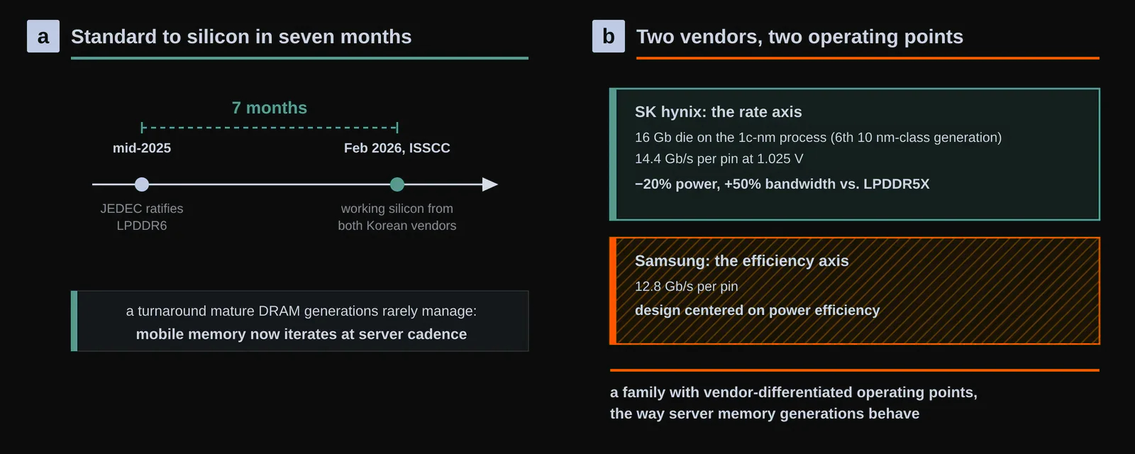
JEDEC ratified LPDDR6 in mid-2025, and by ISSCC in February 2026 both Samsung and SK hynix were presenting functional silicon, a turnaround of about seven months that mature DRAM generations rarely manage. The two implementations split the design space instructively. SK hynix pushed rate: a 16 Gb device on its 1c-nm process (its sixth 10 nm-class generation) running 14.4 Gb/s/pin at 1.025 V, with the company claiming 20% lower power and 50% higher bandwidth against its LPDDR5X[1][7]. Samsung tuned the other axis, presenting LPDDR6 at 12.8 Gb/s/pin with the design centered on power efficiency[2]. Note what the split implies: LPDDR6 is arriving not as one part but as a family with vendor-differentiated operating points, which is how server memory generations behave, not phone memory generations.
The socket problem, solved by a module
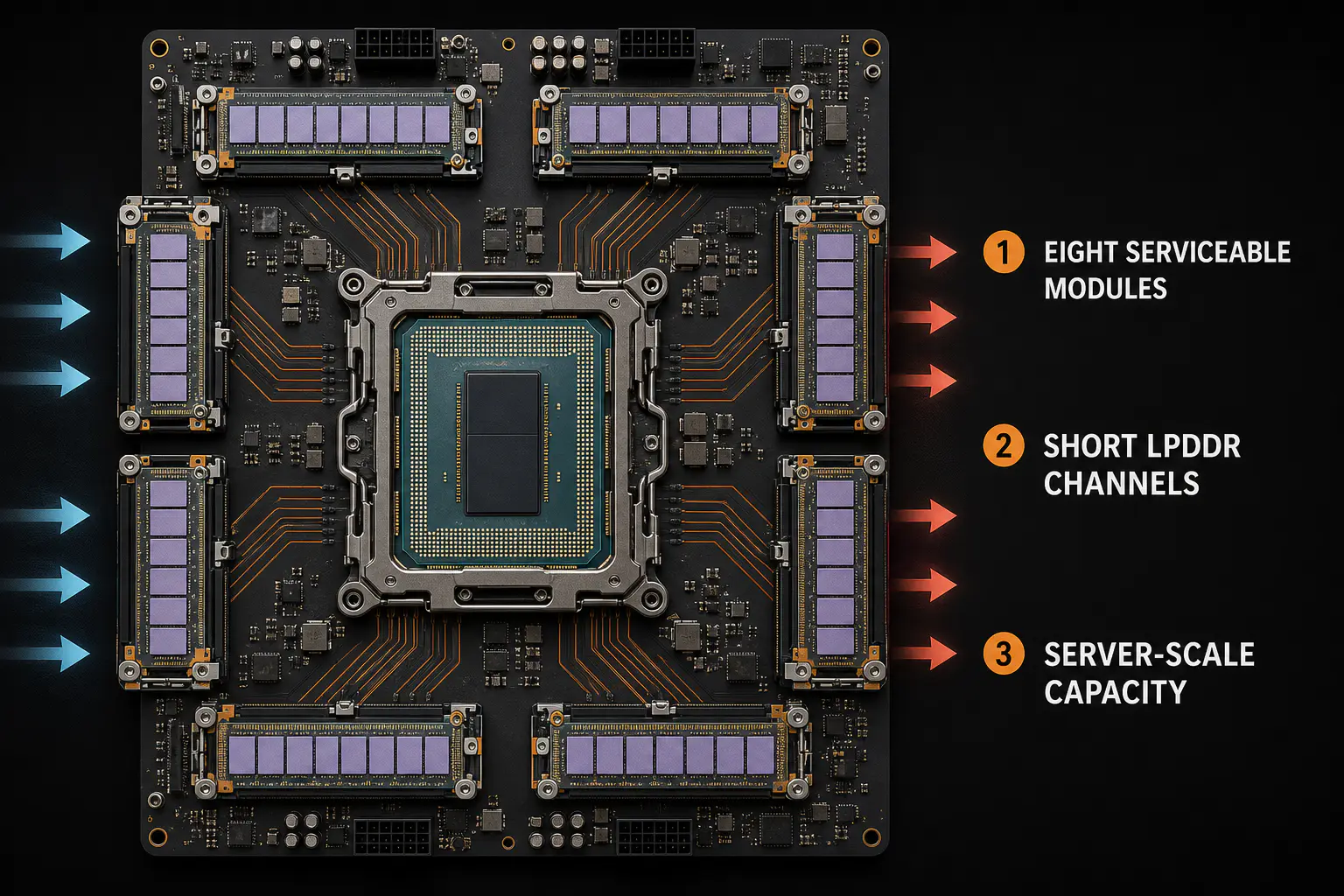
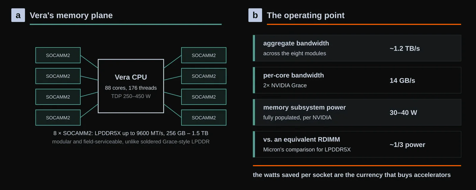
What kept LPDDR out of servers was never speed; it was everything around speed. LPDDR came soldered, so a failed package meant a failed board. Capacity per attachment trailed what stacked RDIMMs offered, and the RAS machinery that datacenter operators trust (spare rows, error telemetry, field-replaceable units) grew up on the registered-DIMM side of the wall. NVIDIA’s Grace crossed the wall anyway by soldering LPDDR5X next to the CPU and accepting the serviceability cost. Vera, detailed at Hot Chips 2026, shows what the second iteration looks like: eight SOCAMM2 module slots per CPU, populated from 256 GB up to 1.5 TB, running LPDDR5X at up to 9600 MT/s for about 1.2 TB/s of aggregate bandwidth, twice Grace’s per-core bandwidth at 14 GB/s per core[3][5].
The power numbers explain the effort, but they need a comparison boundary. NVIDIA’s current Vera architecture page claims up to 1.2 TB/s at half the power of “traditional CPU memory,” together with twice the bandwidth and three times the bandwidth per core of its stated x86 DDR5 baseline[3]. These are vendor system comparisons, not an independent DIMM-to-module laboratory test. Still, the rack-level incentive is clear: power saved on CPU memory can be reassigned to accelerators, cooling or power-conversion margin. SOCAMM restores the modularity half of the RDIMM bargain; the RAS record, which registered DIMMs accumulated over decades, remains the part that only time and published fleet data can supply.
Our separate review, Vera Rebalances the CPU, examines the Olympus core, coherent fabric, benchmark conditions and system-level limits beyond this memory-focused synthesis.
Memory that computes, in a standard package
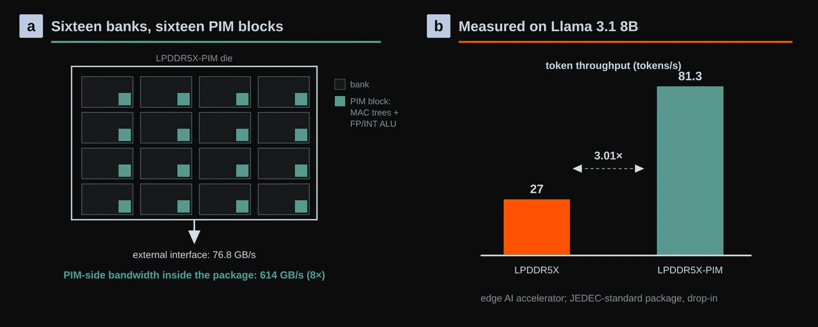
The third announcement moves compute across the interface entirely. Inside any DRAM die, the banks collectively touch far more data per second than the external interface can carry; processing-in-memory (PIM) exploits that gap by planting arithmetic beside the banks. Samsung’s LPDDR5X-PIM, shown at Hot Chips 2026, distributes 16 PIM blocks across the die’s 16 banks, each with multiply-accumulate trees and an ALU handling both floating-point and integer formats, the first low-power PIM part with multi-precision support[4][6]. The internal figure is the story: 614 GB/s of PIM-side bandwidth against 76.8 GB/s through the conventional interface, an 8× gap that never leaves the package. On an edge accelerator running Llama 3.1 8B, token throughput rose from 27 to 81.3 tokens per second, a 3.01× gain, with the decode phase (i.e., the bandwidth-bound phase, as our Raptor coverage discussed) the natural beneficiary.
Two details signal that this is aimed beyond a demo. The part keeps the JEDEC-standard package, so it drops into existing LPDDR5X footprints without board changes. And the standardization machinery is already turning: Samsung and SK hynix are working through JEDEC on LPDDR6-PIM, with Micron also expected to bring PIM to the LPDDR6 generation, which would make computing memory a standard catalog item rather than a proprietary experiment.
What we take from it
Individually, each announcement is incremental: a faster generation, a serviceable module, a lab demonstration. Together they show mobile-derived DRAM taking on server requirements one by one. This does not imply that LPDDR replaces every RDIMM or HBM. HBM still serves the accelerator’s highest-bandwidth tier, while RDIMMs retain mature RAS, broad platform support and large configurations. LPDDR’s near-term opening is the CPU memory plane where bandwidth per watt matters and serviceable modules remove the most obvious operational objection. Three questions remain: fleet-scale error behavior, capacity and upgrade economics against large RDIMM systems, and a PIM programming model that ordinary frameworks can use. The direction is credible because the electrical advantage is real; the market outcome still depends on those system details.
Server LPDDR is a power-and-pin decision
LPDDR reaches high aggregate bandwidth through many narrower channels and lower signaling energy. That can suit a large CPU or accelerator package whose memory controllers sit close to soldered devices or a compact module. The trade is not simply lower power than DDR. Channel count, package and board routing, controller area, command behavior, and service model all change together.
The useful metric is delivered memory work per watt at the system boundary. Measure sustained bandwidth and latency under the intended access mix, then include controller, module, board, and cooling power. A low-voltage interface can save I/O energy while a workload that misses more often or needs additional capacity spends that saving elsewhere. Capacity, bandwidth, and locality must remain attached.
Pin and board efficiency also affect how much memory can surround a socket. More channels can increase concurrency but complicate routing and validation. SOCAMM-style modules attempt to preserve replaceability while using LPDDR components, which shifts mechanical, thermal, and connector constraints rather than eliminating them. Qualification should test every populated channel and the worst supported capacity, not only one favorable module count.
Reliability and serviceability define the server boundary
Phones tolerate soldered memory because the device and memory share a replacement lifecycle. Servers expect error detection, repair, fleet telemetry, field replacement, and years of sustained operation. LPDDR components and modules must therefore be evaluated for the reliability features exposed to the host, how faults are isolated, and what happens when one device or channel degrades.
Error correction can exist on-die, in the memory controller, or across a module-level codeword. These layers protect different faults and expose different telemetry. Corrected-error counts, address isolation, patrol or background checking, and retirement behavior should be visible to fleet management. A system that silently corrects errors without location evidence can preserve data while making predictive replacement harder.
Serviceability has an availability cost. A replaceable module can restore capacity without changing the host, but connectors add signal and mechanical risk. Soldered memory may improve electrical behavior while making a board replacement the repair unit. The total-cost model should include failure rate, spare strategy, repair time, and the amount of healthy compute removed with one memory fault.
Compute inside memory needs a narrow contract
Adding computation near DRAM can reduce movement for operations with high data reuse or simple regular kernels. It can also fragment programming and make memory capacity dependent on a vendor-specific execution path. The interface should expose a small, versioned operation set with explicit precision, ordering, protection, and fallback semantics.
The runtime must decide when offload is worthwhile. Command setup, data layout, synchronization, and result movement can exceed the saved transfer for small or irregular work. A cost model should compare host or accelerator execution with near-memory execution using current queueing and locality. If the operation is unavailable or fails, software should run a correct conventional path.
Security becomes part of the memory contract. Code or commands near memory must obey address protection and tenant isolation, and reset must remove prior state. Attestation and update procedures may be required when the module contains programmable logic. These requirements can determine adoption more than the arithmetic capability itself.
The hierarchy should be designed around workload classes
LPDDR, DDR, HBM, CXL memory, and flash do not form one universal ranking. They trade capacity, latency, bandwidth, energy, persistence, and serviceability differently. A server should place workload classes rather than advertise the sum of all bytes as interchangeable memory.
For each class, record working-set size, access pattern, locality, bandwidth, tail latency, durability, and failure behavior. Then measure completed workload and power as capacity moves between tiers. This reveals whether LPDDR replaces DDR, supplements HBM, or serves a particular host role. The answer can differ between CPU cloud workloads, inference, training input pipelines, and storage services.
We read the rapid progression from standard to silicon and modules as evidence that the server market is exploring a new memory balance. It is not evidence that mobile memory automatically satisfies server operation. The decisive proof will join electrical efficiency with error visibility, repair model, full-capacity qualification, software placement, and useful work per watt over a server lifetime.
Procurement should compare complete memory domains
A fair comparison needs the socket or accelerator, memory controllers, populated capacity, board, cooling, firmware, and operating system. Quoting component pin speed ignores how many channels can run together, how much capacity they provide, and how the platform behaves after one channel is removed. The test should fill the supported memory, exercise mixed read and write traffic, and measure bandwidth, tail latency, power, and corrected errors until temperature stabilizes.
The comparison should include failure and maintenance. Remove or fault one module where the form factor permits it, verify address isolation and retraining, and measure how much compute remains schedulable. For soldered configurations, measure board-replacement time and spare requirements. These tests turn serviceability from a preference into an availability and cost number.
Software qualification is the third layer. Boot firmware, memory training, NUMA discovery, error reporting, virtualization, suspend or reset, and performance counters must describe the new topology consistently. A platform can have efficient devices and still be difficult to operate if firmware hides a weak channel or fleet software cannot distinguish a correctable trend from a sudden failure.
Finally, report the workload crossover. At what working-set size, concurrency, and bandwidth demand does LPDDR-based memory deliver better completed work per watt than the relevant DDR or HBM-backed alternative? Where does capacity, latency, or repair cost reverse the result? A clear non-target region makes the design more credible because it shows that the choice followed measured workload balance rather than a universal memory claim.
The result should be a deployment envelope, not a component verdict. LPDDR6 silicon, SOCAMM2, and memory-side compute expand the options available to system designers. Whether they belong in a given server depends on the combined electrical path, reliability contract, software stack, workload, and replacement model. Those are the conditions under which mobile-derived memory becomes server infrastructure.
Source and attribution
This article is an editorial synthesis prepared for Silicon & Systems. It restates, in our own words, material presented at ISSCC 2026 and Hot Chips 2026, cross-checked against NVIDIA’s current Vera architecture page and the supplemental reporting cited above. Company comparisons are labeled as such and are not treated as independent benchmarks. No source text, table, figure or slide is reproduced, and the figures on this page were created for this summary. The referenced presentations are (c) their respective companies, 2026.