An AI system can contribute to a chip that reaches production without writing the processor’s instruction set, RTL, verification plan or signoff rules. AlphaChip is an important example precisely because its boundary is narrower and its industrial path is longer than the phrase “AI-designed chip” suggests. The system learns to place large circuit components, called macros, on a block floorplan. Conventional electronic design automation (EDA) tools and human engineers still complete the remaining implementation, verification and manufacturing work.
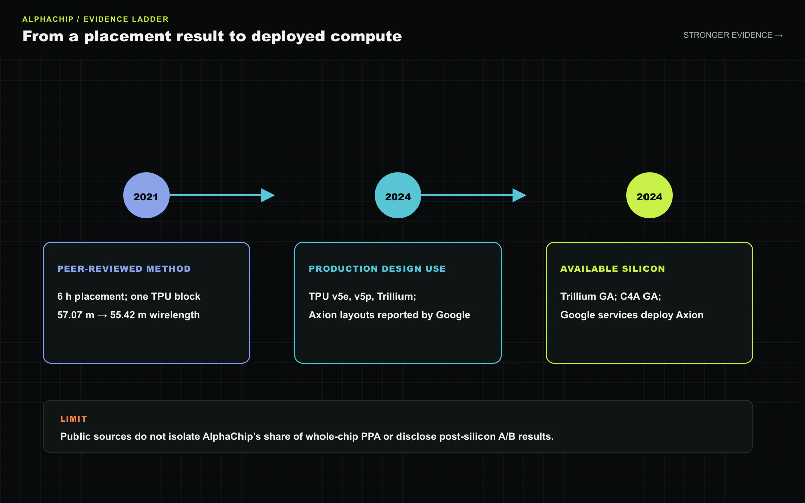
That distinction does not diminish the result. Macro placement is an early physical decision whose consequences propagate into wirelength, congestion, timing, power and the space left for millions of standard cells. A poor arrangement can make downstream closure expensive or impossible. Google reports that AlphaChip-generated layouts were used across TPU v5e, TPU v5p and the sixth-generation Trillium accelerator, and that the technique generated layouts for Axion data-center CPUs[3]. Trillium became generally available to Google Cloud customers in December 2024, while Axion-based C4A virtual machines became generally available in October and were already being deployed by multiple Google services[5][6]. This connects a learned placement method to working, customer-accessible silicon rather than stopping at an academic test.
The public record still leaves a central question: how much of the final chip-level improvement came from AlphaChip? Google provides block-level placement evidence and lists production applications, but it does not publish a controlled post-silicon comparison between the same TPU or Axion design with and without AlphaChip. A technically useful account must therefore keep three claims separate: the method can produce competitive placements, those placements entered production designs, and the resulting processors operate at scale. The sources establish all three, but they do not establish a single causal percentage for whole-chip performance or power.
The physical-design boundary behind the headline
A digital chip begins with architecture and logic intent. RTL describes behavior, synthesis maps that behavior to a gate-level netlist, and physical implementation must place and connect those gates under process, voltage, temperature, timing, power, area and manufacturing constraints. Large memories, data-path arrays and other hard or semi-hard blocks appear as macros. They occupy substantial area, have restricted connection points, and often cannot be reshaped freely. Their locations determine the geometry within which smaller standard cells and routing must fit.
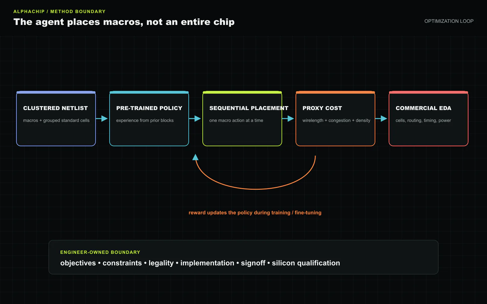
AlphaChip acts at this macro-placement boundary. It receives a clustered netlist in which macros and groups of standard cells form nodes and their connections form edges. Starting with an empty canvas, an agent places one macro at a time. An edge-based graph neural network represents connectivity and helps the policy generalize across blocks. The reward combines proxy wirelength, congestion and density rather than waiting for a manufactured chip. Pre-training on earlier designs provides experience that can be fine-tuned for a new block[1][3].
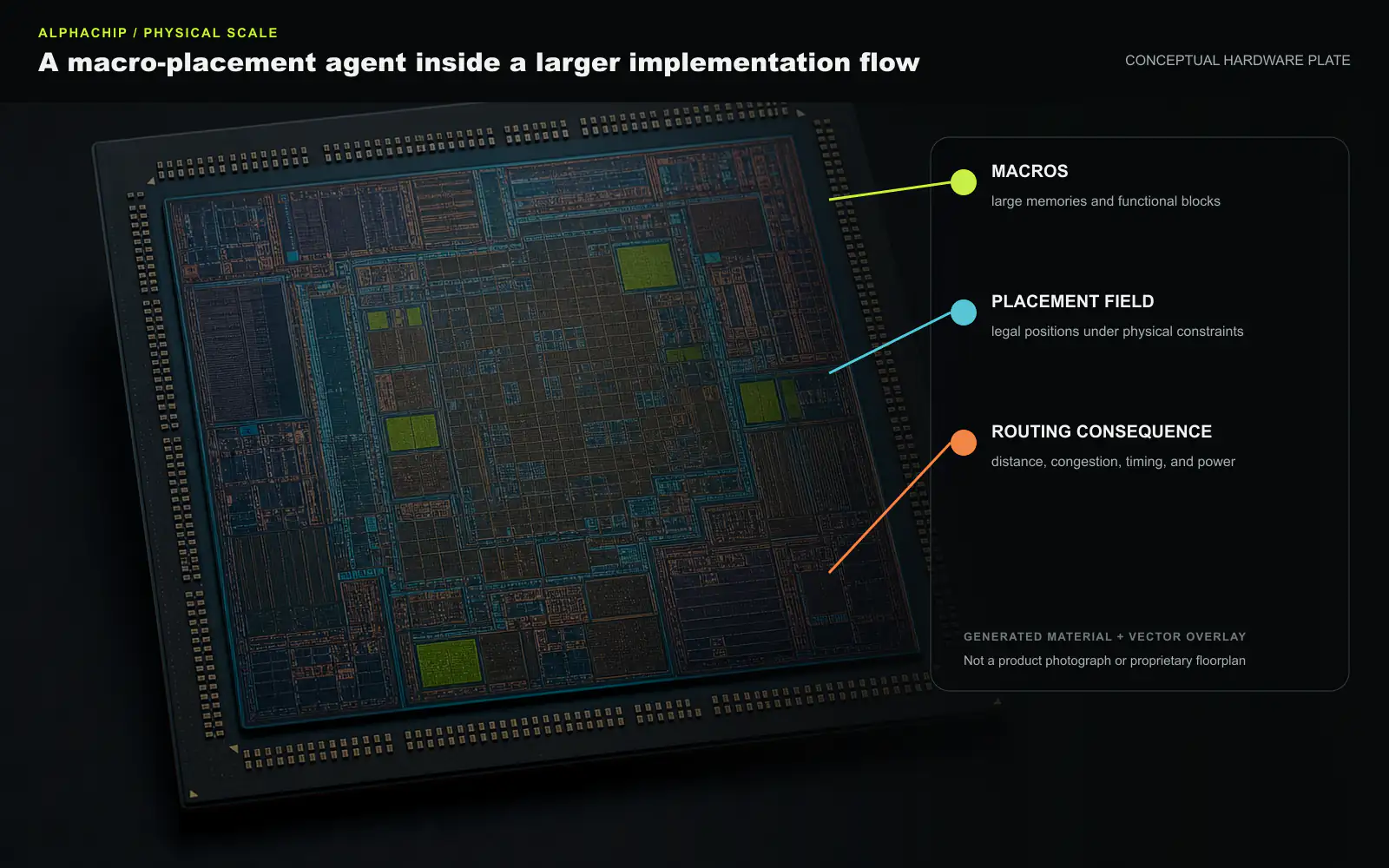
The output is not a finished GDS database. In the evaluation flow described by the Nature paper, each method received the same clustered netlist, macros were placed and snapped to the power grid, and their locations were frozen. A commercial EDA tool then placed standard cells and reported final metrics[1]. Engineers still own placement constraints, power delivery, clocking, detailed routing, static timing analysis, physical verification, design-for-test and functional verification. AlphaChip changes the search over one high-leverage decision layer; it does not remove the implementation flow around that layer.
This boundary also explains why AlphaChip should not be grouped with large language models that generate RTL from a prompt. Its input is a physical connectivity problem, its actions are geometric placements, and its reward encodes implementation proxies. The system is closer to a learned optimizer coupled to EDA than to an autonomous chip architect. As of the sources reviewed here, there is no comparable public primary-source demonstration in which a general-purpose language model generated an entire commercial accelerator’s RTL and the resulting product was independently validated in volume silicon.
What the six-hour result actually measured
The 2021 Nature paper reported that the method could generate a chip floorplan in under six hours and produced results that were comparable or superior to human placements on the reported metrics[1]. For one real TPU block shown in intentionally blurred form, the paper gives 57.07 m of wirelength for the human expert placement and 55.42 m for the learned method. This is a reduction of 1.65 m, or about 2.9%, while the automated run took six hours and the manual baseline took several weeks.
The comparison is meaningful but narrower than a processor benchmark. It evaluates the physical implementation derived from one block-level placement. It does not say that the whole TPU ran 2.9% faster, used 2.9% less energy or cost 2.9% less to manufacture. Wirelength is a useful leading indicator because shorter connections can reduce capacitance, delay and routing pressure, but the final effect depends on buffering, clocking, cell sizing, route detours, voltage choices and many other closure decisions.
The time comparison also needs the correct denominator. “Six hours” refers to generating a placement after the method, infrastructure, cost functions and design representation exist. It does not include the entire development cost of the model, pre-training data, distributed compute environment, EDA integration, constraint preparation or human review. The open-source Circuit Training repository states that the framework can scale distributed collection to hundreds of actors and recommends pre-training on a user’s own chip blocks for the best results[4]. Faster placement for the design team can therefore consume substantial machine time and organizational setup.
This is an exchange, not free automation. Engineering time moves away from manually tuning every candidate and toward defining objectives, curating transferable experience, operating compute, checking legality and interpreting tradeoffs. The economics improve when a team designs many related blocks or generations because the policy and infrastructure can be reused. A single unusual block with limited training data and expensive signoff may see a different balance.
From paper result to three TPU generations
The strongest AlphaChip evidence is continuity. Google DeepMind states that AlphaChip generated layouts used in every TPU generation since the method’s 2020 preprint, specifically identifying TPU v5e, TPU v5p and Trillium[3]. The article says the system first practices on blocks from earlier generations, including on-chip and inter-chip network blocks, memory controllers and data-transport buffers. It then generates layouts for current TPU blocks. Google also states that AlphaChip supplied a larger share of the overall floorplan with each generation.
This repeated use matters more than a one-time benchmark. A production physical-design team is exposed to schedule pressure, late engineering changes, foundry rules and signoff failures that a research benchmark does not reproduce. A method that remains in the flow across three generations has passed an internal economic test: its output was useful enough to review, integrate and carry through the rest of implementation. Reuse also supports the central technical claim that prior placement experience can improve work on related designs.
Trillium provides an external endpoint. Google Cloud announced general availability on December 11, 2024 and stated that Trillium had been used to train Gemini 2.0[6]. Customers could access the same sixth-generation TPU through Google Cloud. The service announcement does not attribute Trillium’s product-level performance to AlphaChip, and it should not be read that way. It establishes that one of the named AlphaChip-assisted generations became operational silicon at cloud scale.
The 2024 addendum to the Nature paper also records the longer deployment claim and gives the method its AlphaChip name[2]. The original article had received a 2023 editor’s note after questions about performance and evaluation. Nature removed that note in September 2024 after post-publication review, stated that the issues had been resolved and closed its investigation while publishing the addendum. This history is relevant because it shows why algorithmic comparisons need disclosed baselines and reproducible evaluation. It does not erase every methodological debate, nor does it negate the documented production use.
Axion strengthens the evidence in a different way
TPUs are closely related accelerator generations, so successful reuse could still reflect a narrow domain. Google says AlphaChip also generated layouts for Axion, its first Arm-based general-purpose data-center CPU[3]. Axion broadens the application from AI accelerators to server CPUs and therefore tests whether the learned placement approach can transfer across a different product class.
Google Cloud made Axion-based C4A virtual machines generally available on October 31, 2024[5]. The announcement says Bigtable, Spanner, BigQuery, F1 Query, Blobstore, Pub/Sub, Google Earth Engine and YouTube Ads had started deploying Axion servers in production. It also made C4A available through Compute Engine, Google Kubernetes Engine, Batch and Dataproc. These facts are stronger evidence of working silicon than a tapeout announcement because customers and internal services execute workloads on the processors.
However, the C4A performance claims are not AlphaChip measurements. Google reports up to 10% better price-performance than recent Arm-based cloud instances and up to 65% better price-performance and 60% better energy efficiency than comparable current-generation x86 instances[5]. Those comparisons reflect the whole Axion platform, including microarchitecture, process, memory, system software, offload and benchmark selection. Public sources do not identify a matched Axion floorplan without AlphaChip. The numbers establish product competitiveness under Google’s stated conditions, not AlphaChip’s isolated contribution.
What production use proves, and what remains private
The evidence can be arranged in ascending strength. A proxy result shows that an optimizer can improve a cost function. A post-route block result shows that the placement survives more of the physical flow. A tapeout shows that the design database was released for manufacturing. Working samples add electrical and functional validation. General availability and production service deployment demonstrate usable systems. AlphaChip reaches the upper rungs because Google identifies products that customers or internal services use.
The missing experiment is a controlled ablation at product level. Ideally, the same block and same downstream tool versions would be implemented from a human baseline and an AlphaChip baseline across multiple seeds, then compared after routing and signoff for frequency, power, area, congestion, runtime and engineer hours. A stronger public record would add yield, silicon frequency distribution, workload energy and schedule effects. Proprietary constraints make that disclosure difficult, but the absence determines what an outside reader may claim.
Another unknown is selection bias. A production team can run the method on many blocks, retain the successful candidates and quietly fall back to manual placement elsewhere. That can still create business value, yet it differs from an algorithm that reliably dominates on every block. Google says AlphaChip contributed more of each successive TPU floorplan, which suggests widening coverage, but it does not publish the denominator of attempted blocks or the rejection rate.
The benchmark baseline also changes with time. Human experts use modern analytical placers, internal scripts and prior-generation templates; they do not arrange every macro by hand on a blank canvas. A fair comparison is therefore not AI against unaided humans. It is an AI-assisted flow against the best established human-and-tool flow, with equal compute budgets and the same final signoff. The Nature evaluation tried to standardize key downstream conditions, while the production record supplies a different kind of evidence: teams kept the method because it fit their operating process.
The system lesson is reusable search, not human removal
The AlphaChip case changes the design-management question. Macro placement was historically a scarce-expert loop: choose a layout, run expensive implementation, inspect congestion and timing, revise constraints, and repeat. A learned policy can turn prior blocks into a starting point and generate candidates while engineers focus on the objective and the difficult exceptions. The gain comes from searching more of a structured space within a schedule.
That value compounds when three conditions hold. First, the organization has a stream of related designs, so pre-training experience transfers. Second, the downstream flow can evaluate candidates consistently; a noisy or changing reward teaches the wrong preference. Third, compute is available early enough that broad exploration does not delay signoff. When these conditions fail, the policy can optimize proxies that do not survive routing or consume more infrastructure than the saved engineering time justifies.
Governance also moves upstream. If a reward underweights timing risk, power-grid access or a rare physical rule, the agent can systematically propose attractive but costly candidates. Teams need versioned constraints, held-out blocks, seed variation, regression against the incumbent flow and a record of which suggestions were accepted. A model checkpoint becomes part of the implementation toolchain and should receive the same configuration control as scripts, libraries and EDA versions.
For chip companies evaluating AI placement, the most useful procurement questions are operational. Which stages are automated, and which metrics are proxies? Does the result include placement only, post-route signoff, tapeout or measured silicon? How many blocks were attempted, accepted and manually rescued? What compute and license hours produced the result? Can models transfer across blocks without leaking proprietary design data? What happens after a process-design-kit or tool-version change? A percentage improvement without these labels is difficult to budget.
AlphaChip is therefore neither proof that AI can autonomously create a processor nor merely a laboratory curiosity. It is evidence that a learned optimizer can enter a high-value physical-design loop, accumulate reusable experience and contribute to processors that operate in cloud services. The careful conclusion is narrower than the headline and more consequential for engineering: the successful unit of automation was a well-defined search problem embedded in a conventional signoff organization.
Sources and copyright notice
This is an independent Silicon & Systems analysis based on the 2021 Nature paper, its 2024 addendum, the Google DeepMind production account, the open-source Circuit Training repository, and Google Cloud announcements for Axion C4A and Trillium general availability. The Nature article and addendum are © Springer Nature 2021 and 2024. No source figure is reproduced. All figures were created for this article; generated material plates are explicitly labeled and do not depict a proprietary product or floorplan.