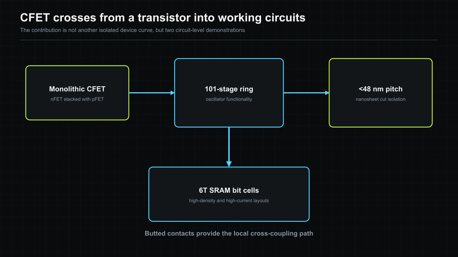
A stacked transistor becomes a logic technology only when it can drive a circuit. TSMC’s earlier monolithic CFET work placed an nFET over a pFET at a 48 nm gate pitch. Its IEDM 2025 paper takes the next step: a fully functional 101-stage ring oscillator and operational 6T SRAM bit cells at a pitch below 48 nm[1]. The shift from device curves to feedback and memory circuits is the reason this result matters.
The two test vehicles ask different questions. A ring oscillator connects many inverters in a loop, so one weak isolation boundary, contact or stage can prevent oscillation. A 6T SRAM cell packs two cross-coupled inverters and access devices into a layout where matching and local wiring are inseparable from transistor behavior. Demonstrating both means the CFET process supports repeated logic and a compact state-holding circuit, not merely one vertical transistor pair.
Isolation turns devices into a chain
TSMC introduces nanosheet-cut isolation (NCI) to separate neighboring devices inside the ring oscillator. The need is straightforward: vertically stacked channels save area, but lateral leakage or an incomplete cut between adjacent structures can break the intended inverter chain. The 101-stage oscillator therefore tests whether the isolation method can be repeated across a circuit long enough to sustain feedback.
The public program states that the design uses a nanosheet-based monolithic CFET flow and reduces gate pitch below 48 nm[2]. It does not disclose oscillator frequency or stage delay in the abstract. That omission limits performance conclusions. Functionality proves connectivity and switching; it does not by itself show that the stacked circuit beats a nanosheet CMOS baseline in power, speed or yield.
SRAM makes the local interconnect visible
SRAM is a more severe density test because its cross-coupled inverters require short local connections. TSMC reports two butted-contact (BCT) variants that provide those connections in high-density and high-current cell designs[1]. The contact is not a secondary packaging detail. Once nFET and pFET sit on different vertical levels, the way their terminals meet can determine whether the theoretical transistor footprint survives in the completed cell.
Two cell variants expose the design trade-off. A high-density cell prioritizes area, while a high-current cell reserves more electrical strength. Presenting both suggests that CFET design will need a library of device and contact options rather than one universal layout. This resembles current standard-cell practice, but the vertical dimension adds alignment, parasitic and process-variation constraints.
The paper describes the cells as operational and identifies them as the smallest SRAM bit cells in the authors’ comparison set[1][2]. We retain the scope of that claim. The public materials do not provide an array size, bit yield, read margin distribution or retention data. A single working bit cell is a circuit milestone; a dense SRAM macro needs redundancy, peripheral circuits and statistical yield.
What changed at IEDM 2025
CFET discussions often start with an area sketch: place complementary devices vertically and recover the width previously occupied by one polarity. TSMC’s result moves the discussion to the objects that surround the devices. NCI must create clean circuit boundaries. BCT must connect inverter nodes. The process must repeat across 101 stages and support two SRAM layouts. These are the mechanisms that determine whether vertical stacking reaches a real cell.
The next evidence should quantify the benefit after wiring. Ring-oscillator energy and delay need comparison at matched voltage and drive. SRAM needs array-level yield, read and write margins, leakage and cycling data. Standard-cell demonstrations need routed block results because local density can be lost in contacts or higher metal layers. Backside power delivery may relieve some routing pressure, but it adds another integration stack.
Our reading is that TSMC has crossed an important boundary from device feasibility to circuit feasibility. It has not yet crossed from a conference test vehicle to a product-qualified logic platform. That distinction does not diminish the result. It tells us exactly what the next publication must prove.
Why 101 stages are more informative than one inverter
An inverter can switch even when its parasitics, contact resistance or threshold balance are unsuitable for a useful library. A ring oscillator multiplies these weaknesses. Its oscillation period contains the delay of every stage, and a defective open or short anywhere in the loop can stop the circuit. Reaching 101 stages therefore tests repeatability across many CFET pairs and local connections on one path.
The result still needs a denominator. Oscillation establishes that the loop has gain and a finite delay, but the public abstract does not state frequency, supply voltage, load or power. Without those conditions, stage delay cannot be compared with a planar or nanosheet reference. The same device can appear fast at a higher voltage while losing the energy advantage expected from density scaling. A complete result would report delay and energy at several voltages, plus the distribution across devices and wafers.
NCI also deserves attention as a design rule rather than a named module. The cut must terminate adjacent nanosheets without consuming the pitch saved by stacking. Its overlay and etch margin determine how closely cells can abut. If the isolation requires a large keep-out area, the process can demonstrate a narrow gate pitch yet deliver a wider standard-cell footprint. Electrical isolation, printability and layout density must therefore be evaluated together.
The two SRAM cells reveal a library decision
High-density and high-current cells are not redundant demonstrations. They expose the fact that CFET SRAM will need distinct ratios among pull-up, pull-down and access devices. A compact cell can minimize footprint but leave less current margin during write. A stronger cell can improve access or stability while spending area, capacitance or leakage. Vertical stacking does not remove these circuit ratios; it changes the geometries and contacts used to realize them.
The butted contact is central because a 6T cell contains cross-coupled internal nodes. Those nodes must connect devices that occupy different vertical tiers without taking a long detour through upper metal. A local vertical connection can preserve density, but its resistance and capacitance enter both read and write timing. Alignment error may also affect the two sides of the cell differently. Reporting two BCT variants implies that the contact is part of circuit optimization, not a fixed back-end detail.
Operational bit cells answer only the first memory question. A usable array needs word-line and bit-line drivers, sense amplifiers, precharge circuits, redundancy and error repair. Bit-line capacitance can dominate the access energy that was invisible in a single cell. Statistical read and write margins must cover process, voltage and temperature corners. Thus, the smallest working cell does not automatically produce the smallest reliable macro.
Monolithic stacking changes the thermal and process budget
Monolithic CFET forms the complementary devices within one tightly coupled process sequence. That approach can align the tiers more closely than bonding two finished wafers, but the lower device experiences the operations used to create the upper one. Dopant activation, epitaxy, dielectric formation and metal work functions must fit a shared thermal budget. A process improvement for one polarity can narrow the margin of the other.
Self-heating also changes when active channels sit vertically. Heat from the lower device must pass through surrounding dielectrics and the upper structure before reaching some heat-removal paths. In a sparse test oscillator the average power may be modest, while a dense logic block or SRAM array can sustain simultaneous activity. Compact models will need tier-aware thermal resistance so timing analysis can capture temperature-dependent mobility and leakage.
Reliability follows the same geometry. Gate dielectric aging, contact electromigration and dielectric breakdown can have different stress conditions by tier. A shared local connection can turn one weak interface into a cell failure. Product qualification will require accelerated stress across multiple circuit patterns rather than a lifetime extrapolated from isolated transistors.
Samsung and TSMC demonstrate different maturity steps
Samsung’s 42 nm 3DSFET result and TSMC’s sub-48 nm CFET circuits should not be ranked by pitch alone. Samsung emphasizes six-channel device integration, controlled epitaxy and middle isolation at the tighter reported pitch. TSMC emphasizes circuit closure through a long oscillator and two SRAM cells. One provides stronger evidence at the device-process boundary; the other advances further into local interconnect and circuit behavior.
Together they show the sequence required for a platform. Device electrostatics must survive vertical integration, contacts must preserve the footprint, repeated cells must switch, and arrays and routed blocks must meet distributions. No single conference vehicle covers all four. A customer should therefore ask which layer of evidence a CFET announcement supplies instead of treating every demonstration as equivalent.
What would establish product relevance
The next decisive disclosure would combine a characterized standard-cell library with an SRAM macro on the same flow. For logic, placed-and-routed benchmark blocks should report area, frequency, dynamic energy and leakage against a current GAA baseline. For memory, the evidence should include array dimensions, bit yield, read and write margins, retention and error-repair assumptions.
Manufacturing data must accompany circuit data. Useful items include critical-dimension and overlay distributions, contact resistance by tier, defect maps, and performance across multiple wafers. Thermal measurements should cover sustained activity rather than only short functional tests. These are demanding requirements, but they are the evidence needed to justify the added process modules.
TSMC’s IEDM work matters because it removes one common objection: vertically stacked complementary devices can form repeated feedback logic and state-holding cells below a 48 nm gate pitch. It does not yet establish competitive power, speed, density after routing or array yield. The correct conclusion is circuit feasibility with a clearly defined path to platform qualification.
Source and copyright notice
This article is an independent editorial summary of TSMC’s IEDM 2025 paper and official conference abstract. We used the public research record only to establish context and restated the technical content in our own words. No source text, circuit layout, table or figure is reproduced. The explanatory figure was created specifically for this article. The conference paper is (c) IEEE 2025.