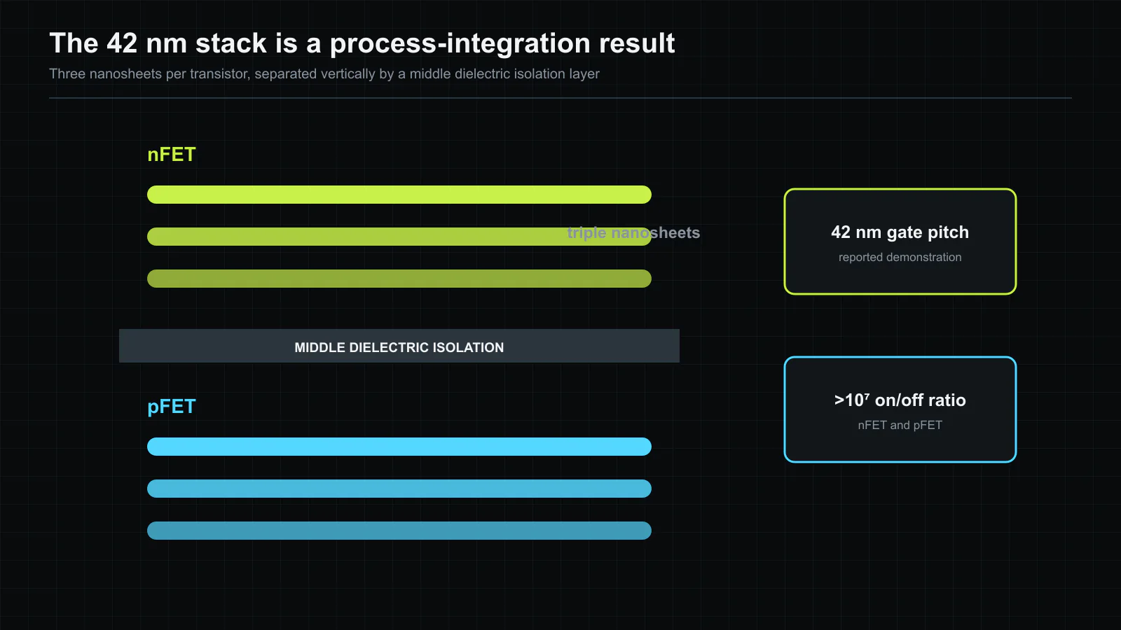
The next density step is no longer only about making one transistor narrower. A standard CMOS cell places n-type and p-type devices beside each other, so both consume lateral width even when each channel is already a gate-all-around nanosheet. Samsung’s VLSI 2026 paper changes that arrangement: three nanosheets form the upper nFET, another three form the lower pFET, and the pair fits into a reported 42 nm gate pitch[1]. This is the vertical complement to gate-all-around scaling.
The achievement should be read precisely. Samsung demonstrated individual stacked devices with current control and wafer-level uniformity. It did not present a complete standard-cell library, an SRAM macro, or product yield. The important evidence is that the process steps needed to build the stack were implemented together on an industrial wafer flow.
Why three plus three matters
Stacking devices saves footprint only if each device still carries useful current. A single narrow nanosheet would concede drive strength while reducing area. Samsung instead uses three channels for each polarity, preserving effective channel width in both the upper and lower transistors. The reported subthreshold swings are 75 mV/dec for the nFET and 73 mV/dec for the pFET, while both on/off current ratios exceed 10^7[4]. Those figures show switching behavior on both levels of the stack rather than a structural cross-section alone.
The 42 nm gate pitch makes integration harder. Source and drain regions, gates, contacts and isolation all compete for a smaller horizontal distance, while the upper device must also align to the lower one. Thus, the paper’s core contribution is not the drawing of a stacked FET. It is the process sequence that produces two controllable transistor tiers at an aggressive pitch.
Epitaxy and isolation carry the result
Two process details decide whether the stack works. First, repeated epitaxial growth must create uniform silicon channel layers without allowing accumulated defects to disturb the upper sheets. Samsung reports an optimized process that suppresses cross-hatch defects and improves channel uniformity[2]. The challenge is statistical: a six-sheet vertical structure is only useful when variation remains controlled across many devices.
Second, the middle dielectric isolation (MDI) layer must electrically separate the upper and lower transistors while leaving enough room to form different gate stacks. Samsung uses epitaxial layers with three germanium concentrations to position the MDI accurately[1]. A misplaced or nonuniform boundary can couple the tiers or complicate the work-function materials needed for nFET and pFET threshold control.
These details also explain why a stacked FET cannot be judged only by its footprint. Vertical density transfers difficulty from lithographic width into epitaxy, selective removal, material interfaces and three-dimensional variability. The area benefit is real only if those steps meet manufacturing yield and reliability targets.
What the paper proves, and what it does not
The work proves that triple-nanosheet devices of both polarities can be vertically integrated at 42 nm pitch and electrically characterized on the same wafer. The VLSI program selected it as a technology highlight, and Samsung reports an 8.29/10 review score among more than 1,000 submissions[2][3]. Those facts establish technical interest, not product readiness.
The next evidence should come from circuits. Ring oscillators would expose accumulated delay and variability. SRAM cells would test local interconnect, matching and read stability. Standard cells would reveal whether vertical contacts and routing actually reduce cell area after design rules are applied. Thermal coupling, reliability and repair strategy will also matter once many stacked pairs switch together.
Our conclusion is therefore narrower than the phrase “future logic” may suggest. Samsung has shown that vertical nFET/pFET integration can move from a conceptual device into an industrial process demonstration. The remaining question is whether the contacts and wires around that device preserve the density advantage at circuit scale. That is the line separating a transistor milestone from a technology platform.
The process sequence creates coupled constraints
The vertical stack cannot be fabricated as two independent transistors that are simply joined at the end. Channel epitaxy, source and drain formation, sacrificial-layer removal, MDI placement and gate replacement constrain one another. A selective etch that improves access to the lower sheets can also disturb the upper device’s support structure. Likewise, a thermal step used after the lower transistor is formed must stay within the material budget of the layers already present. This coupling is why a six-sheet cross-section is evidence of process integration rather than only device geometry.
The three germanium concentrations are especially important in that sequence. Germanium content changes the etch selectivity of SiGe against silicon, allowing a chosen layer to define the eventual dielectric boundary while adjacent layers retain their intended role. The method gives the process more than one chemical marker along the vertical direction. However, every composition transition introduces another interface whose thickness, roughness and strain can vary. Production control therefore needs inline metrology that can infer buried-layer placement before the completed device reaches electrical test.
Upper and lower source/drain formation creates a second dependency. The bottom device must receive a low-resistance junction without allowing the later upper-tier operations to degrade it. Conversely, etching toward the lower tier must not create leakage paths through the middle isolation. The paper’s electrical results show that these steps can coexist in a test flow. They do not yet report contact resistance distributions for a routed cell, which will be necessary to translate channel current into useful circuit current.
Density must be measured after contacts and power delivery
CFET density claims often begin with the observation that vertical stacking can remove one transistor row from a cell. That is a geometric upper bound. A finished standard cell still needs gate contacts, upper and lower source/drain contacts, signal pins, local interconnect and access to the power rails. If those structures require additional horizontal keep-out zones, the cell-width reduction can be smaller than the device footprint suggests.
Backside power delivery is one possible complement. Moving the power rails below the device can free front-side routing tracks and provide a shorter path to the lower transistor. It can also make the lower contact scheme and wafer handling more complicated. A fair comparison should therefore hold the logic function, drive strength, routing rules and power architecture constant. Reporting only gate pitch compares one dimension while leaving the cell-height and wiring problem unresolved.
This distinction also separates Samsung’s result from a block-level performance, power and area claim. A process can support a 42 nm gate pitch while a useful library chooses a looser pitch to improve yield or pin access. Designers will need multiple cell heights and drive-strength options, and the densest cell may not be the one used on critical paths. The relevant metric is placed-and-routed block area at a stated timing and power target.
Variability becomes vertical as well as lateral
Conventional within-die variation already includes line-edge roughness, metal-gate work-function variation and local source/drain resistance. A stacked pair adds correlations between tiers. A thickness shift in the epitaxial stack can change both channel dimensions and the MDI position. Upper-tier processing can create a different thermal and stress history from the lower tier. Thus, the two transistors in one logical inverter may not vary independently.
The reported subthreshold swings and on/off ratios establish usable electrostatics, but distributions matter more than representative values for a large circuit. SRAM would be an exacting test because read stability depends on ratios among several devices. Logic timing would expose the tail of slow stages across thousands of cells. Reliability experiments should also separate bias-temperature instability, hot-carrier aging, dielectric breakdown and thermal coupling by tier rather than reporting one aggregate lifetime.
Yield introduces another multiplication. If a critical defect opportunity exists in each sheet or interface, six vertically aligned channels give more places for a local failure to invalidate the pair. That does not imply that CFET yield must be poor. It means defect density, redundancy and repair cannot be inferred from a working device population alone. Wafer maps over multiple lots will be more informative than another isolated best curve.
The decisive experiment is a routed logic block
A credible next sequence would begin with inverter and NAND/NOR cells, continue through ring oscillators and SRAM arrays, and end with a synthesized block. Each stage answers a different question. Small cells test contact topology; oscillators expose accumulated delay; arrays expose matching and bit yield; a routed block measures whether pin congestion and upper-metal use preserve area savings.
The comparison should include a contemporary non-stacked GAA baseline fabricated with similar materials and contacted design rules. Useful reporting would provide frequency at matched voltage, energy per transition, leakage per cell, active area after routing, and distributions across wafers. Thermal maps under sustained switching would show whether the upper device impedes heat removal from the lower one. Those measurements would convert the 42 nm device milestone into a technology assessment.
Samsung has therefore answered the first manufacturing question: can six nanosheet channels, two threshold polarities and an isolation boundary be integrated at this pitch with controlled switching? The answer is yes for the demonstrated vehicles. The harder commercial question is whether that vertical complexity buys block-level density after contacts, power and yield are counted. Until those data appear, 3DSFET should be treated as a strong process candidate rather than a finished node.
Source and copyright notice
This article is an independent editorial summary of Samsung Electronics’ VLSI 2026 paper, the official conference material and Samsung’s public technical explanation. We restated the mechanisms, measurements and limitations in our own words. No source sentence, table, micrograph or figure is reproduced. The explanatory figure was created specifically for this article. The conference paper is (c) IEEE 2026, and the company material is (c) Samsung Electronics 2026.