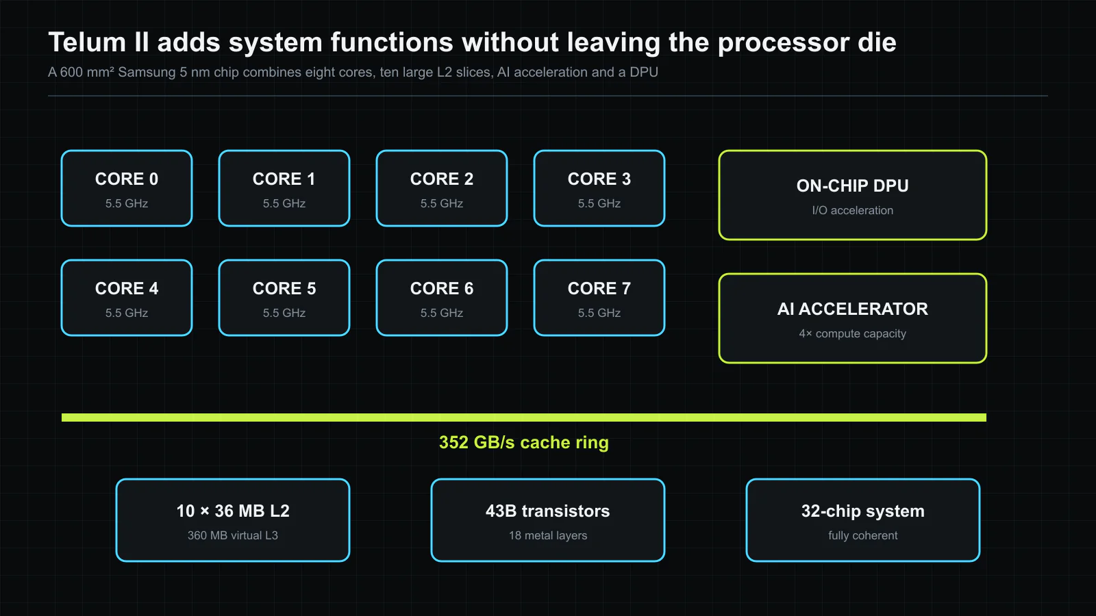
Telum II is a processor only if the word includes much of the system. IBM’s 600 mm² die contains eight 5.5 GHz cores, ten 36 MB L2 cache slices, a second-generation AI accelerator and a new data processing unit for I/O acceleration. Built in Samsung’s 5 nm bulk process, it carries 43 billion transistors, 165 billion vias and more than 24 miles of wire across 18 metal layers[1]. The numbers describe a design whose main challenge is coordination, not merely core throughput.
IBM built Telum II for the z17 mainframe, where a drawer contains eight processor chips and a maximum system connects 32 chips into one coherent memory domain. That context determines the architecture. Transaction latency, cache capacity, cryptography, I/O and availability must improve together, while the power profile remains within 5% of the previous generation[2][3].
Cache is the scale-up fabric on the die
Each of the eight cores and the DPU receives a private 36 MB L2 slice, and a tenth floating slice increases usable capacity. A 352 GB/s ring connects the ten slices. IBM’s virtual-cache scheme allows the aggregate 360 MB to act as an on-chip shared L3, while a populated drawer exposes 2.88 GB as virtual L4[1]. Compared with the previous Telum generation, on-chip cache capacity rises by 40%.
The cache increase is not simply a larger die. IBM reports a 20% core-area reduction obtained through microarchitectural and physical-design changes, including removal of two levels of physical hierarchy inside the core. A high-density Samsung SRAM cell then provides more cache per area. The result keeps eight cores while creating room for two functions that previously lived elsewhere: stronger AI acceleration and an I/O DPU.
The DPU moves into the coherence boundary
The new DPU initially accelerates complex I/O protocols for networking and storage. Integrating it on the processor die gives the unit coherent access to the cache hierarchy and removes a separate chip boundary for selected operations. IBM reports a 50% increase in I/O density at the system level[4]. However, the public paper does not reduce the DPU to a generic SmartNIC comparison. Its benefit belongs to IBM Z’s protocol stack, reliability model and drawer topology.
The same qualification applies to AI. IBM states that the integrated accelerator provides four times the compute capacity of the previous Telum chip[4]. In z17, the company positions that hardware for in-transaction inference, where a fraud or risk model executes inside the response path rather than sending data to a remote accelerator. IBM later reported a system capability of more than 450 billion inference operations per day at one-millisecond response time[5]. These are product workload claims, not a substitute for model-by-model throughput and accuracy results.
Physical design carries architectural intent
Running a large die at 5.5 GHz while adding 40% more latches requires the clock and voltage networks to absorb substantial variation. Telum II uses a resonant clock mesh over most of the die, separate asynchronous meshes for memory and PCIe, and an on-chip voltage-control loop. The loop adjusts dynamic voltage without forcing every workload to operate at a higher fixed voltage[1]. IBM reports that the overall power profile stays within 5% of the prior generation even as frequency and capacity increase[2].
The metal stack also reveals where advanced processor scaling now goes. Eight narrow layers serve local interconnect, eight medium-width layers carry performance-sensitive routes, and two ultra-thick layers handle off-chip signaling plus power and clock distribution[1]. Transistor count alone cannot describe this die. Its performance depends on delivering power, clock and coherent data across an area approaching the reticle limit.
A specialized answer to a general trend
Telum II should not be judged as a general-purpose server CPU entering a core-count race. IBM chose eight high-frequency cores and invested the remaining transistor and wiring budget in cache, AI, I/O and system coherence. That decision follows the workload: financial and enterprise transactions value low latency, data locality and continuous operation more than a large pool of independent cores.
The broader lesson is that system boundaries keep moving onto silicon. A cache ring becomes a local fabric, a DPU enters the processor, and AI inference sits beside the transaction cores. This integration can reduce latency and data motion, but it also makes the chip more specialized. Telum II is therefore evidence for both sides of advanced silicon economics: integration creates system value, and that value is strongest when the vendor controls the hardware, operating system and workload stack together.
Scale-up changes what a private cache means
The labels L2, virtual L3 and virtual L4 describe one physical cache resource at different scopes. A core’s nearby slice supplies the low-latency path, while address and coherence mechanisms let unused capacity in other slices act as a larger logical cache. Extending the abstraction across eight chips in a drawer increases the data that can remain near the processors without presenting software with a collection of unrelated caches.
This organization trades simple locality for managed sharing. A request that misses its local slice may traverse the on-die ring, and a drawer-level access must cross chip boundaries. The system therefore needs policies that place frequently used lines close enough while retaining aggregate capacity. The 3.6 ns L2 latency reported for the journal version is a local property; it is not the latency of every access to the virtual hierarchy[3]. Performance depends on the hit distribution across those scopes.
The floating tenth slice gives IBM another control point. It adds capacity without belonging exclusively to one core or the DPU, which can reduce imbalance when a workload’s footprint is uneven. However, arbitration and quality of service become important when transaction cores, AI inference and I/O processing contend for the ring. A capacity number alone cannot show whether a latency-sensitive core is protected from a burst generated by another agent.
The drawer is the real unit of architecture
Telum II enters the system through dual-chip modules. Four such modules populate a drawer, producing eight processor dies; four drawers yield the 32-chip maximum described by IBM. This packaging hierarchy is not an implementation footnote. It determines hop count, cache scope, bandwidth, failure containment and service procedures.
A mainframe must continue operating through component faults and maintenance events. Consequently, off-chip links need redundancy, error detection and recovery behavior that consumer benchmark summaries rarely expose. Capacity that exists only when every link is healthy would not meet the platform’s availability objective. IBM’s design choices should be interpreted against this requirement: predictable recovery and data integrity can justify area or latency that looks inefficient in a throughput-only comparison.
The hierarchy also explains why 352 GB/s on the on-die ring is not a system bandwidth claim. Traffic between slices uses that local fabric, while drawer and multi-drawer transfers follow other links and protocols. An application sees the composition of all these paths. Useful workload analysis should separate local-cache hits, remote-slice hits, chip-to-chip traffic and memory accesses rather than dividing one advertised bandwidth by the core count.
AI and I/O share silicon but not necessarily objectives
In-transaction inference favors a different operating point from batch accelerator throughput. The model must complete inside a service response budget, often on data already protected and formatted by the transaction system. Avoiding an external accelerator can save serialization, network and queueing time even when a separate device offers more arithmetic throughput. Telum II’s AI block should therefore be evaluated by end-to-end latency, supported models, numerical formats and accuracy constraints.
The DPU has another workload. It handles selected I/O protocol work so cores can spend fewer cycles moving or transforming data. Coherent cache access can reduce copies, yet the DPU’s requests consume ring and cache resources. The architectural question is not whether either accelerator is fast in isolation. It is whether admission control and prioritization preserve transaction latency when the CPU, AI engine and DPU operate together.
IBM’s public fourfold AI-capacity and 50% I/O-density claims use product-level baselines[4]. They are valuable for generation-to-generation planning, but they do not establish portability to another server architecture. The comparison includes software, topology and workload choices that IBM controls. That vertical control is an advantage of the platform and also the reason the figures should not be converted into generic accelerator rankings.
Power delivery and clocking limit the large die
A 600 mm² die at 5.5 GHz has spatially different voltage droop, temperature and process speed. Raising the global voltage to satisfy the slowest region would waste power across the rest. The on-chip control loop instead observes operating conditions and adjusts voltage dynamically. Its benefit depends on response time and stability: correction must be fast enough for workload changes without creating oscillation or timing uncertainty.
The resonant clock mesh recovers part of the energy normally spent charging a large clock network, but resonance works over a designed frequency range and physical load. Separate asynchronous meshes for PCIe and memory let those regions use their own timing domains rather than forcing one clock solution across the die. Crossing between domains then requires synchronization and verification. Clock efficiency is achieved through more explicit domain management, not by making timing complexity disappear.
Ultra-thick upper metals carry power and global signals because local interconnect dimensions are poorly suited to low-resistance distribution across the die. Those layers compete for routing resources and must tolerate current density over long product lifetimes. The reported 165 billion vias show how many vertical transitions connect the stack. Via resistance and redundancy are therefore system reliability concerns, not only layout statistics.
How to judge Telum II fairly
Generic core benchmarks would reveal part of the picture but miss the main design objective. A fair assessment would use mixed transactional workloads with encryption, database access, inference and I/O, then report tail latency, throughput, energy and recovery behavior. Measurements should identify how often data is served by each cache scope and whether accelerator traffic changes the tail of CPU response times.
Availability needs explicit tests as well. Link degradation, cache-slice errors and accelerator faults should be injected while the system remains under load. The useful result is not simply that an error was detected, but how much capacity and latency changed during recovery. These experiments connect the physical reliability features to the service-level promise of the platform.
Telum II is notable because IBM spent advanced-node area on functions that make a 32-chip machine behave as one managed system. The design does not imply that every server processor should integrate the same blocks. It shows that when a vendor controls packaging, firmware, operating system and transaction software, moving AI and I/O into the coherence boundary can be more valuable than adding another group of general-purpose cores.
Source and copyright notice
This article is an independent editorial summary of IBM’s ISSCC 2025 papers, the related journal record and official IBM product materials. We separated conference measurements from company workload claims and restated the architecture in our own words. No source sentence, die photograph, table or figure is reproduced. The explanatory figure was created specifically for this article. The conference paper is (c) IEEE 2025, and the company material is (c) IBM 2024-2025.