An accelerator package can have enough total cooling capacity and still fail at one square millimeter. A logic die stacked above a small active die sends concentrated heat through bumps, underfill, organic build-up layers, and copper wiring before that heat can use the package footprint. IBM’s ECTC 2025 work asks a focused question: can the substrate itself become a lateral heat spreader without becoming an electrical short?[1]
The proposed answer is a graphite sheet embedded near the top of an organic substrate. Graphite conducts heat unusually well along its plane, yet poorly through its thickness. That anisotropy is useful when the problem is a hot spot that must spread sideways before it travels into the board or cooling structure. It is also dangerous because graphite conducts electricity. The paper therefore treats insulation and via placement as part of the thermal architecture, not as post-processing details.
The bottleneck begins below the die
Conventional package discussions often start with a lid, thermal interface material, and cold plate. Those elements dominate a top-side heat path, but a stacked die can place a hot component below another die or behind a restricted vertical path. The local temperature then depends on how quickly heat can leave the small footprint before the surrounding material becomes a thermal bottleneck.
Organic substrates contain copper planes and vias, but they are designed primarily for power and signals. Adding thermal copper can compete with routing, create stress, and still provide only discrete vertical paths. IBM instead uses a continuous sheet to collect heat laterally. The sheet is not a replacement for the cold plate. It is an intermediate layer that enlarges the effective area seen by the remaining cooling path.
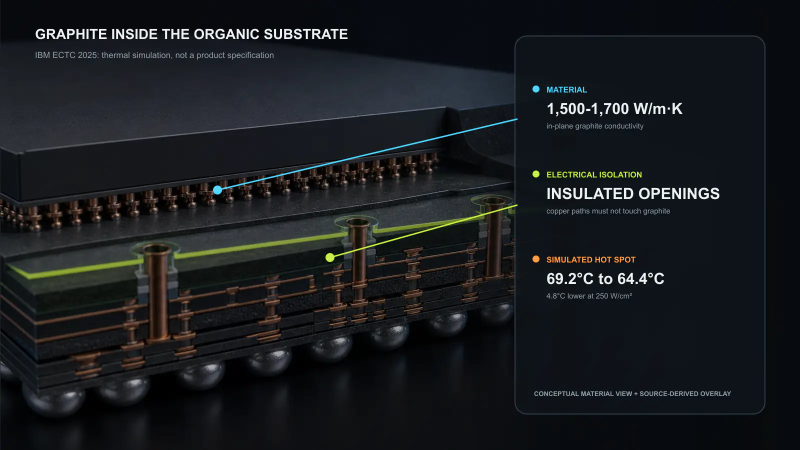
The reported graphite has an in-plane thermal conductivity of 1,500 to 1,700 W/m·K and a through-plane value of only 5 to 7 W/m·K. The ratio is the mechanism. Heat entering one region can move across the sheet readily, while the sheet itself does little to conduct heat through its thickness. Placement close to the source therefore matters more than simply adding graphite somewhere in the laminate.
Electrical isolation defines the manufacturable topology
A graphite layer cannot cross power and signal vias as if it were an inert dielectric. Any exposed contact can form an unintended conductive path. IBM’s structure therefore creates openings through the sheet, insulates their inner walls, and routes the vertical connections through those isolated holes. The package gains lateral thermal continuity while preserving electrical separation.
This requirement changes the optimization problem. A larger graphite area spreads heat better, but every via opening removes material and adds an interface that must survive fabrication. Dense power delivery and high-speed escape routing can perforate the very sheet intended to spread heat. Conversely, routing around graphite can lengthen electrical paths. Thermal, signal, and power design must share one keep-out map.
The concept also depends on edge control. Graphite particles or exposed sheet edges cannot be allowed to contaminate build-up processes or create leakage. Lamination pressure, resin flow, drilling, desmear, plating, and registration all become part of the isolation system. The paper reports fabrication and thermal, mechanical, and electrical evaluation, but a product decision still needs defect distributions and lifetime data rather than a nominal cross section alone.
One simulation shows the scale of the benefit
IBM highlights a two-chip stack whose upper die measures 20 mm on each side and produces 250 W/cm². A lower die measuring 0.5 mm on each side sits at its center. In this modeled configuration, the modified structure reaches a 64.4°C maximum, 4.8°C below the 69.2°C baseline. The reduction is meaningful because it comes from redistributing a concentrated source rather than lowering total package power.[1]
The result should not be generalized into a fixed percentage for every package. The boundary conditions, cooling surfaces, graphite dimensions, interface resistances, and location of the heat source determine the gain. A uniformly heated large die may see less benefit because it already uses much of the package area. A small buried hot spot can see more value because lateral spreading attacks the dominant geometric constraint.
The first-author IBM technical article later discusses a broader double-sided cooling concept and reports up to a 20% reduction in temperature rise for a related simulated structure.[2] That number is not the ECTC paper’s 4.8°C result. It combines a power insert and a wider cooling topology. Keeping the two evaluations separate matters because a substrate graphite sheet and a complete double-sided cooling architecture have different assembly requirements.
Anisotropy is both the advantage and the limit
High in-plane conductivity makes graphite effective only when heat can enter and leave the sheet through acceptable interfaces. A poor bond between the hot region and the graphite adds contact resistance before lateral spreading begins. After spreading, heat still needs a path from the sheet into a board, stiffener, heat sink, or bottom-side cooling component. The through-plane value of 5 to 7 W/m·K prevents the sheet from acting like an isotropic copper slab.
Thickness introduces another trade-off. A thicker sheet can carry more lateral heat, but consumes substrate thickness and can intensify mechanical mismatch. A thinner sheet fits more easily yet may be disrupted by openings and local processing. The correct comparison uses sheet conductance, which combines conductivity and thickness, together with interface resistance and the fraction of area removed for vias.
Graphite orientation must also remain controlled. The reported conductivity assumes the preferred planes run in the desired lateral direction. Wrinkles, cracks, resin intrusion, or local delamination can interrupt that path. A coupon measurement of pristine material is not enough to describe the embedded layer after package processing.
Reliability can erase a thermal win
Organic laminate, copper, graphite, underfill, and silicon expand differently with temperature. The embedded sheet changes local stiffness and can move neutral axes in the substrate. Thermal cycling may concentrate stress around insulated openings, while moisture can alter resin properties and interfacial adhesion. A design that lowers peak silicon temperature but creates via cracking or leakage is not a system improvement.
The required qualification therefore spans electrical isolation resistance, dielectric breakdown, via-chain continuity, warpage, peel strength, thermal cycling, humidity bias, and power cycling. It should compare substrates with and without graphite using the same routing density and assembly flow. Measurements need spatial resolution because an average package temperature can hide the local hot spot the sheet is designed to relieve.
Inspection is equally important. Manufacturers need to detect sheet misregistration, damaged insulation, voids, and exposed edges without destroying the package. X-ray imaging may reveal metal geometry but not every graphite-resin defect. Acoustic microscopy, electrical test structures, and sectioned process monitors may need to work together.
The package-level decision is a routing decision
This approach is most attractive when three conditions coincide: the source is spatially concentrated, a lateral area exists to absorb the spread heat, and the via map leaves a continuous graphite path. AI and HPC packages with stacked logic, local power-delivery hot spots, or asymmetric chiplet activity can meet those conditions. A conventional single large die with a strong top-side cold plate may not.
Design teams should begin with the transient power map, not the graphite data sheet. They need to identify how long each hot spot persists, whether neighboring regions heat at the same time, and where the spread heat can exit. A sheet that merely moves heat into an already hot memory stack or voltage-regulator region can reduce one sensor reading while worsening another limit.
Electrical co-design follows immediately. Power vias have limited freedom, high-speed channels require reference continuity, and package escape routes impose density. The remaining connected graphite area determines thermal effectiveness. Thus, the most useful design artifact is a combined heat-flow, via, and isolation map rather than separate thermal and electrical drawings.
Transients decide how much spreading is useful
A steady-state map does not describe every accelerator workload. Matrix engines can switch from a low-power synchronization phase to a dense compute phase within milliseconds, while memory and I/O regions follow different duty cycles. A graphite sheet begins redistributing heat immediately, but the silicon, substrate, board, and cooling assembly each have their own thermal time constants. The measured benefit therefore depends on pulse duration and repetition as well as average power.
Short bursts may be absorbed partly by the local thermal mass before the spread heat reaches a remote sink. Long phases approach the reported steady condition and make the exit path from the graphite more important. Repeated bursts can raise the baseline temperature until the package behaves like a continuous load. A qualification vehicle should reproduce all three regimes instead of applying one constant heater pattern.
Transient measurements also reveal whether the sheet moves a hot spot or actually lowers the system limit. Infrared thermography can observe accessible surfaces, while embedded diodes or resistance sensors can track buried regions. Calibrated structure functions can separate interface and bulk resistances. The experiment should record the coolest and hottest regions simultaneously so a lower peak at one die is not purchased by heating another component.
Workload scheduling could eventually use this information. If graphite couples two regions thermally, running their peak phases together may be worse than alternating them. Package telemetry and runtime placement then become part of the value proposition. That conclusion cannot be derived from the ECTC simulation alone, but it identifies the system experiment needed after the material concept is proven.
What evidence would justify production use
The ECTC result establishes physical plausibility and gives a concrete simulated operating point. Production adoption needs measured temperature maps on assembled test vehicles across multiple power patterns. The baseline should include optimized copper-only substrates so the comparison does not reward graphite for solving an avoidable routing problem.
Yield data should report sheet registration, isolation defects, via opens, and delamination by lot. Reliability should show whether thermal benefit remains after cycling and moisture exposure. System tests should measure sustained frequency, leakage, board temperature, and cooler requirements. A 4.8°C reduction matters most if it preserves clock frequency, lowers fan or pump power, or expands allowable ambient temperature.
Cost must include substrate processing, inspection, lost routing area, and qualification. Graphite is not valuable merely because its conductivity is high. It is valuable when the complete insulated layer lowers the cost of meeting a thermal limit more than an alternative such as a vapor chamber, thicker copper, backside power delivery, or a different die placement.
What we take from it
IBM’s work moves thermal design into a layer that package architects normally reserve for wiring. The result is not a universal graphite recipe. It is a method for matching an anisotropic material to a geometric hot-spot problem while treating electrical isolation as the enabling structure. The 4.8°C simulation is a credible reason to build and test the idea, not permission to skip routing, reliability, and boundary-condition analysis.
For AI and HPC packaging, the larger lesson is that cooling no longer ends at the lid. When stacked and disaggregated dies create small buried heat sources, organic substrates may need to route heat alongside power and data. The winning solution will be the one that preserves those three networks together.
Source and copyright notice
This article is an independent editorial digest written in our own words from the official IBM Research record, the ECTC program, and an IBM technical article by the first author. No sentences, figures, or tables from the IEEE paper are reproduced. The figure was created for this article from reported facts and clearly separates a conceptual material view from deterministic labels. The conference paper is © 2025 IEEE. IBM’s technical article remains © IBM. The DOI above links to the original record.