Wafer flatness is becoming an active process variable in advanced packaging. Hybrid bonding, wafer-to-wafer alignment, temporary carriers, backside processing, and thick redistribution layers all assume that the wafer stays within a narrow shape window. A film added for electrical or mechanical reasons can bend a 300 mm wafer enough to break that assumption. Evatec’s IMAPS Device Packaging Conference paper treats deposited stress as a control input rather than an unwanted residue.[1]
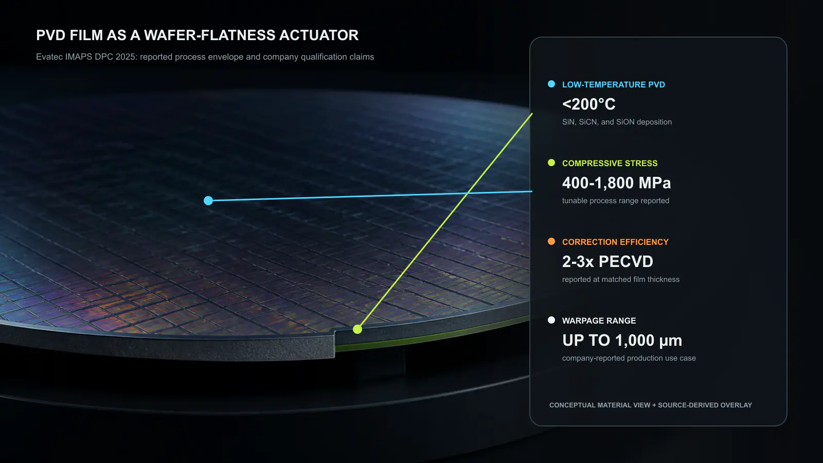
The presentation connects two related uses of low-temperature physical vapor deposition (PVD). Silicon carbon nitride (SiCN) provides a hybrid-bond dielectric or surface layer at temperatures below 200°C. Silicon nitride (SiN) and silicon oxynitride (SiON) provide controlled compressive stress on the backside to correct bow. One process family therefore addresses the bonding interface and the geometry needed to bring that interface into contact.
Hybrid bonding needs more than a small pitch
Hybrid bonding joins dielectric surfaces and embedded copper contacts with little or no conventional bump height. Fine pitch reduces interconnect length and capacitance, but it also removes the compliance that solder bumps provide. Particles, local topography, wafer bow, and film stress can prevent simultaneous contact across the wafer. The alignment tool may place two wafers correctly while their surfaces still fail to meet.
The dielectric must be deposited within the thermal budget of completed devices and temporary materials. Evatec reports PVD SiN and SiCN processes below 200°C. The SiCN examples include 50 nm films deposited at 113°C and 152°C. These temperatures are relevant because packaging stacks can contain polymers, copper structures, and devices that cannot tolerate a front-end furnace cycle.
Low temperature does not automatically guarantee a bond-ready surface. Composition, density, roughness, moisture uptake, plasma damage, and surface activation determine whether two films bond and whether the interface remains stable. The public paper emphasizes deposition capability and outgassing behavior rather than a complete copper-dielectric hybrid-bond yield study.
Outgassing evidence is useful but qualitative
The authors use flash thermodesorption spectroscopy from room temperature to 900°C at a 20°C/min ramp. Signals from the reported PVD SiN and SiCN films remain near a background level around 1.0 × 10⁻¹¹ in the plotted data. They describe the films as showing no outgassing.
That result supports clean downstream processing, but the public slides also state that exact mass-spectrometry values could not be measured. The correct interpretation is therefore background-limited qualitative evidence, not a universal numerical upper bound. Film area, chamber history, detection sensitivity, gas species, and storage conditions would be needed to compare the process with another supplier quantitatively.
Adhesion is similarly conditional. An inductively coupled plasma etch pre-clean improves adhesion on the organic material used in the test. The presentation reports no delamination on silicon wafers and attributes that behavior partly to closer thermal expansion. It does not establish adhesion across every polymer, metal, cleaning sequence, or humidity condition used in packaging.
Film stress becomes a wafer-shape actuator
Any deposited film stores stress. If a compressive film sits on one side of a wafer, the film and substrate seek different in-plane lengths and the composite bends. Process engineers normally try to minimize this effect. Evatec instead tunes the stress and thickness so that the new curvature opposes the wafer’s existing bow.
The reported 300 mm production configuration supports thick films in the 2 to 5 µm range. The presentation shows compressive-stress control over roughly 400 to 1,800 MPa, with some process plots emphasizing about 600 to 1,800 MPa. It also reports stress above 1.2 GPa for both SiN and SiON. These values should be read as process ranges from the vendor’s equipment and examples, not guaranteed material constants.
Curvature depends on more than stress. Film thickness, wafer thickness, elastic moduli, temperature, radial uniformity, and the starting shape all matter. A nominally identical average stress can produce different local geometry if the film is thicker at the edge or if the wafer begins with saddle-shaped distortion. The deposition system must therefore control spatial stress as well as the wafer average.
The reported correction reaches severe warpage
Evatec claims correction or control of up to 1,000 µm of wafer warpage and describes a qualification at a major 3D NAND manufacturer. It also reports two to three times greater warpage-correction efficiency than plasma-enhanced chemical vapor deposition (PECVD) at matched film thickness. These are consequential production claims because a more efficient film can use less thickness or correct a more severe incoming shape.
The comparison needs its conditions. PECVD and PVD films can differ in composition, density, hydrogen content, modulus, stress stability, and uniformity. A ratio at matched thickness does not by itself predict final yield. The more useful metric is the fraction of wafers that enter the next tool’s chucking and alignment window after deposition and remain there through subsequent thermal cycles.
The public paper does not provide the sample count, incoming bow distribution, edge exclusion, within-wafer stress map, corrected-wafer yield, or long-term stability behind the 1,000 µm statement. We therefore treat it as a vendor-reported capability rather than independently reproduced evidence.
Saddle correction requires spatial control
A wafer does not always bend as a simple bowl. Asymmetric stacks, patterned films, and carrier release can create a saddle with opposite curvature along two axes. A uniform backside coating cannot fully cancel that shape because it applies nearly axisymmetric stress.
Evatec presents sector-based stress engineering as a feasibility path. The illustrated range extends from about +150 MPa tensile to -600 MPa compressive in selected regions. By changing stress azimuthally, the process can add different bending moments along different directions. This is closer to shape correction than average bow compensation.
Patterned stress introduces new controls. Sector boundaries can create local curvature gradients, wafer handling may rotate the error relative to the pattern, and overlay between the measured shape map and deposition recipe becomes critical. Production use needs a closed loop: measure the wafer, calculate the required stress field, deposit it with known transfer behavior, and verify the result.
Stress can move instead of disappear
Flattening the wafer at room temperature does not eliminate stored energy. It redistributes stress across silicon, films, metal, and interfaces. When the wafer is heated for bonding, cured, thinned, diced, or released from a carrier, moduli and thermal expansion change. A wafer that is flat at metrology temperature can bow again at the bond temperature or after singulation.
High compressive stress can also promote buckling, cracking, edge delamination, or particle generation. Thick 2 to 5 µm films add deposition time and cost. If the film remains in the product, its electrical, moisture, and thermal behavior become part of package qualification. If it is removed, the temporary correction must persist long enough to complete the critical process.
Thus, the target is not minimum bow at one step. It is a shape trajectory that stays within every downstream tool window while preserving interface and device reliability. The recipe should be optimized against that sequence.
AI and HPC make the geometry harder
Large interposers, chiplet arrays, HBM stacks, backside power structures, and thick redistribution layers produce asymmetric material stacks. AI and HPC packages also push reticle and panel dimensions, so a small curvature per unit length becomes a large edge displacement. Fine-pitch bonding then has less mechanical compliance to absorb the error.
This is why wafer-flatness control belongs in package architecture. A designer who adds a thick copper layer, a low-loss dielectric, or a backside structure also changes the stress budget. Waiting until bonding to address the resulting bow can force a costly carrier or reduce usable area. A controllable backside film offers another actuator, but it needs to be planned alongside the layers that create the distortion.
SiCN links this geometric problem to bonding. If the same low-temperature PVD platform can provide a suitable dielectric surface and stress-control films, a manufacturer may simplify thermal-budget management and tool integration. That is an operational hypothesis. The paper does not quantify cross-contamination, throughput, maintenance, or cost of ownership for the combined flow.
The control loop determines line value
Stress correction becomes operationally useful only when metrology and deposition form a stable feedback loop. The line first needs a repeatable full-wafer height map with a coordinate reference. A model converts that shape into a target stress and thickness field. The deposition tool applies the recipe, and a second measurement estimates the residual error. Recipe learning must distinguish a systematic tool signature from product-to-product variation.
This loop has a time budget. A high-resolution scan, recipe calculation, thick-film deposition, and verification step can consume more line time than a passive carrier solution. If every wafer needs an individual map, metrology capacity may set throughput. If one recipe serves a lot, incoming variation may reduce correction yield. The economically correct granularity could be product, lot, or wafer, and the public paper does not determine it.
Control stability also matters. Correcting the measured residual too aggressively can make the next iteration overshoot, particularly when film stress drifts with target age or chamber condition. Statistical process control needs reference wafers, target-life tracking, and alarms for spatial modes that the recipe cannot correct. A saddle pattern and a uniform bowl should not be collapsed into one bow number.
The best production metric is not deposited stress. It is downstream tool availability and bonded good area per hour. A process may use a thicker film and still win if it prevents chucking failures or edge voids. Another may produce an impressive flatness map yet lose on cycle time, particles, or rework. These measurements translate Evatec’s material leverage into a factory decision.
What a procurement-quality evaluation needs
A useful qualification should start with incoming wafer-shape maps across several product stacks, not blank silicon alone. It should report bow and local height before deposition, after deposition, at bond temperature, after bonding, and after reliability stress. The dataset needs wafer count, edge exclusion, film uniformity, and failed-wafer distributions.
Hybrid-bond evaluation should add surface roughness, bond wave propagation, void density, copper contact resistance, dielectric breakdown, alignment yield, and thermal cycling. Outgassing should be measured with calibrated species and detection limits. Adhesion should cover the actual polymer and cleaning sequence used in production.
For shape control, the comparison with PECVD should hold film thickness, starting geometry, and downstream thermal history constant. Cost should include deposition time, target utilization, chamber cleaning, metrology, recipe computation, and any removal step. Only then can a 2 to 3× stress efficiency be translated into line capacity or yield.
What we take from it
Evatec’s central idea is stronger than a list of coatings: film stress can be an intentional actuator that prepares a packaging wafer for fine-pitch bonding. Low-temperature SiCN addresses the interface, while stressed SiN or SiON addresses whether the surfaces can meet across 300 mm. The reported ranges show that PVD has enough leverage to matter.
The evidence boundary is equally important. This is an industry proceedings presentation with vendor data, not a public multi-lot yield study. The 1,000 µm correction and 2 to 3× efficiency claims justify a product-specific evaluation. They do not establish universal superiority. Package teams should judge the method by the complete wafer-shape trajectory and bond yield, not by stress magnitude alone.
Source and copyright notice
This article is an independent editorial digest written in our own words from the official IMAPSource proceedings PDF. No sentences, figures, or tables are reproduced. The figure was created for this article and labels vendor-reported values explicitly. The original proceedings material is © 2025 IMAPS and its authors. The DOI above links to the source record.