Commercial AI-assisted electronic design automation has crossed an important threshold: the public record contains named semiconductor companies, production design flows and tapeouts rather than only anonymous benchmark blocks. Synopsys said DSO.ai had participated in its first 100 commercial tapeouts by February 2023[1]. Cadence told investors in April 2025 that Cerebrus had been used in well over 1,000 tapeouts[7]. Samsung, STMicroelectronics, SK hynix, MediaTek, Renesas and Samsung Austin have disclosed results or production use.
Those statements do not mean that an AI system autonomously conceived and built one thousand chips. The tools operate mainly inside digital implementation. They search combinations of tool settings, constraints, floorplan choices and implementation recipes, evaluate power, performance and area (PPA), retain promising runs and send selected designs through established signoff. Architecture, RTL intent, verification, process rules, product qualification and most exception handling remain engineering responsibilities.
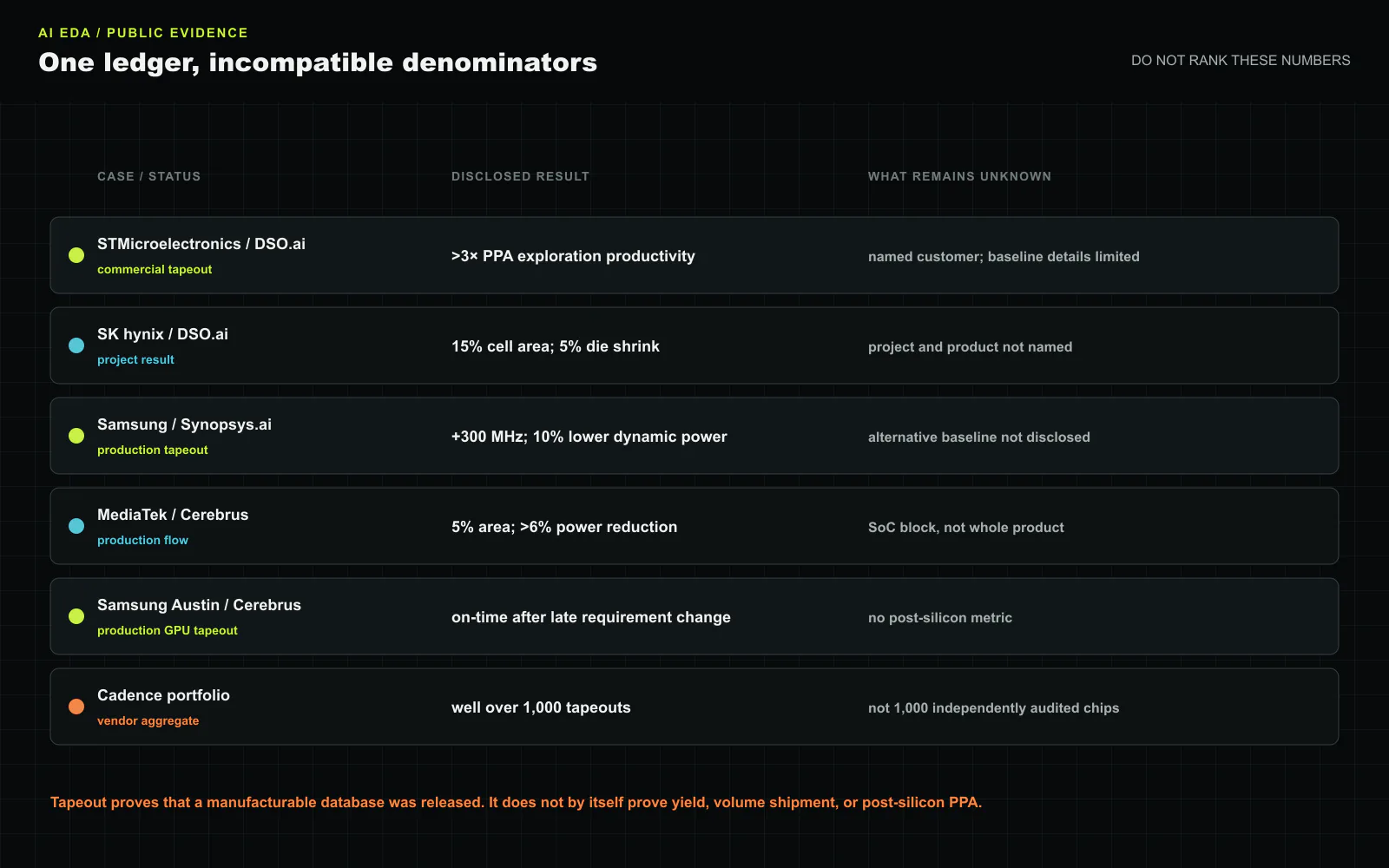
The evidence is also heterogeneous. A 5% die reduction on an unnamed project cannot be ranked against 300 MHz more frequency on a mobile CPU or a portfolio count of tapeouts. “Production flow” can mean that a tool is approved and repeatedly used, while “production tapeout” means that manufacturing data for a design was released. Neither phrase by itself confirms acceptable yield, volume shipment or measured performance in packaged silicon. This article builds an evidence ledger rather than a vendor scorecard.
The operating model: replace serial tuning with managed search
Physical implementation contains a large number of interacting choices. Synthesis effort, placement density, timing targets, clock options, buffering, power optimization, routing effort and floorplan dimensions can each change the result. A manual team develops a known-good flow, launches runs, waits for reports, compares outcomes and changes a small number of settings. Advanced-node designs add more corners and constraints, while a single full-flow experiment can consume substantial compute and licenses. The schedule limits how much of the space engineers can inspect.
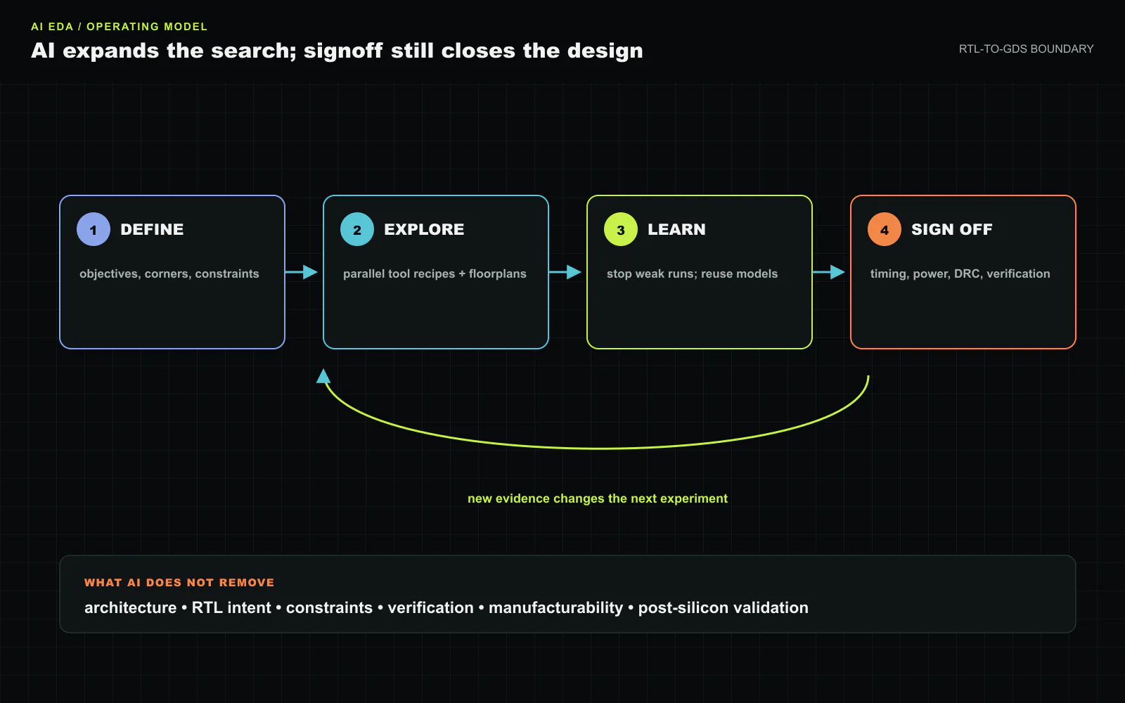
Synopsys DSO.ai and Cadence Cerebrus turn this process into a managed search. The optimization layer proposes implementation configurations, distributes runs and learns from the resulting PPA or schedule objectives. Cadence describes a reinforcement-learning engine that samples design data while runs execute, stops candidates that are not converging and reallocates compute to other configurations[4]. Its model can be reused as a starting point for related projects. Synopsys similarly describes reinforcement learning over large design spaces connected to Fusion Compiler and IC Compiler II[1].
This is valuable because the optimization knobs are coupled. A setting that improves timing can increase power or congestion; shrinking a floorplan can reduce area until routing detours erase the gain. The AI system does not need to discover a new transistor or write a new CPU pipeline to create value. It needs to test more combinations than a team can examine manually and find a design that satisfies the specified objective before the tapeout deadline.
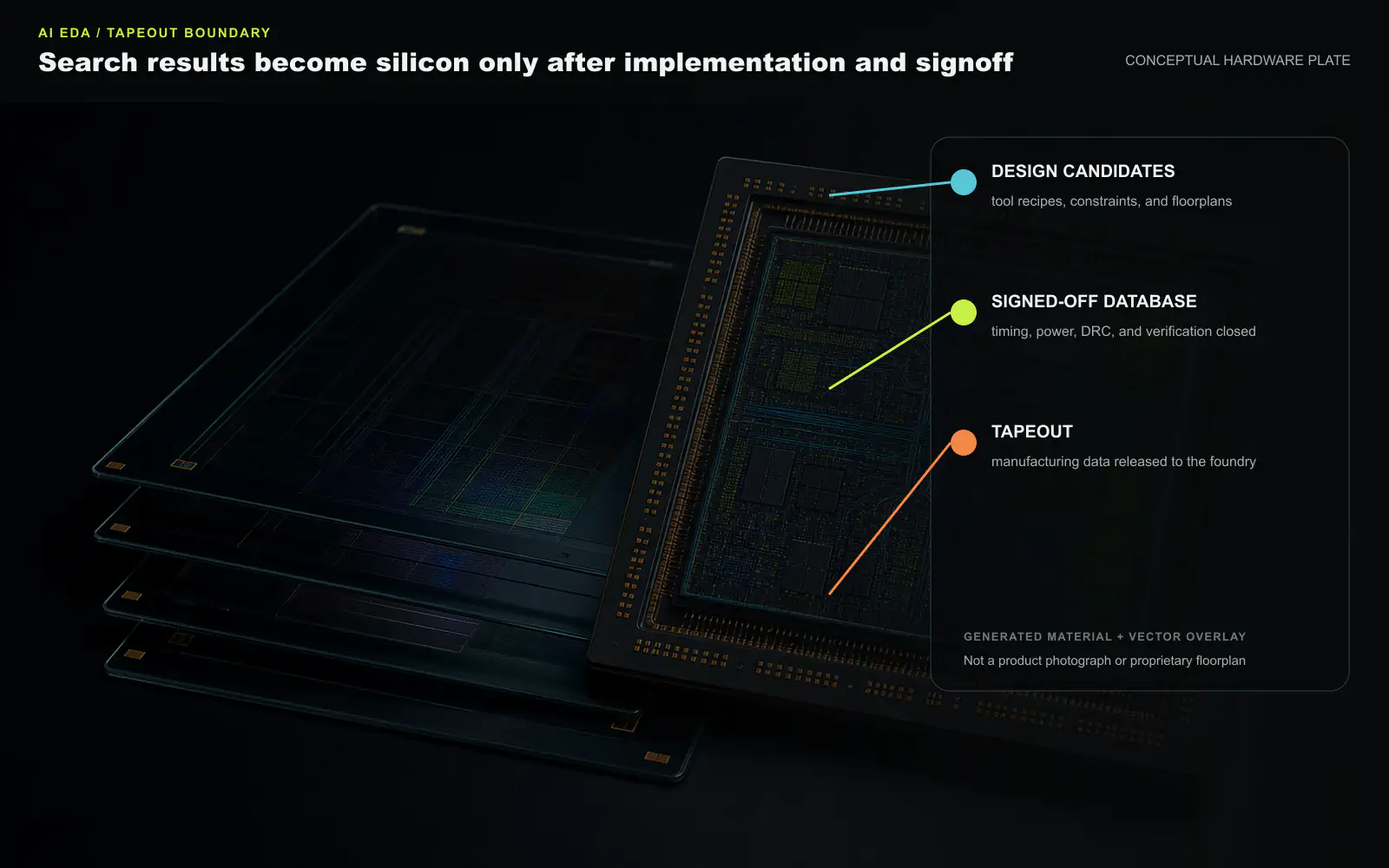
Compute becomes an explicit input. Parallel exploration can reduce calendar time while increasing total machine and license consumption. The correct productivity metric is therefore not only engineer days. It includes wall-clock time to an acceptable design, compute-hours, license-hours, cloud transfer and storage, failed runs, review time and the quality of the selected result. Vendor releases often report the first and last terms but do not disclose the full resource denominator.
The objective is another engineering artifact. If a reward favors nominal frequency but underweights hold closure, voltage-drop risk, congestion tails or a difficult operating corner, the search can produce a strong headline and a weak implementation. Teams must define legal bounds, preserve signoff independence and test whether the learned preference transfers after a process-design-kit or EDA version change. AI increases the number of experiments; it does not redefine manufacturability.
Synopsys: 100 tapeouts with two quantified customer cases
Synopsys’s February 2023 release is useful because it separates a portfolio milestone from named examples[1]. The company said customers had reached 100 commercial tapeouts with DSO.ai. Across customer results since launch, it reported more than 3× productivity, up to 25% lower total power and die-size reductions. These are aggregate upper-bound statements. They are not one matched result achieved on every tapeout.
STMicroelectronics provides a more specific boundary. ST used DSO.ai on Microsoft Azure together with Synopsys physical-implementation tools and completed what the release calls the first commercial design tapeout using AI in the cloud. ST reported more than a 3× increase in PPA exploration productivity while implementing a new Arm core and exceeding its PPA goals. The design team and application are named, but the release does not publish the exact core, process, before-and-after PPA values, compute budget or post-silicon measurement.
SK hynix reported a different project result: a 15% cell-area reduction and a 5% die shrink[1]. Cell area and die area are not interchangeable. Standard cells occupy only part of a die alongside memories, analog blocks, I/O, whitespace and routing. A 15% reduction in the optimized cell region translating to 5% at die level is physically plausible and shows why the measurement boundary matters. The project and product are not identified, and the announcement does not state whether the values are pre-route, signoff or measured silicon.
In May 2024, Synopsys and Samsung announced a production tapeout for a high-performance mobile SoC on Samsung Foundry’s gate-all-around process[2]. The release says the design included flagship CPU and GPU work and reports 300 MHz higher performance and 10% lower dynamic power than alternative approaches. It identifies Fusion Compiler, DSO.ai and a broader Synopsys.ai stack. However, the “alternative approaches” baseline, absolute frequency, voltage, workload and post-silicon status are not disclosed. The result supports production implementation on an advanced process, not a general 300 MHz expectation for other designs.
Synopsys said in March 2024 that its AI-driven EDA suite had enabled hundreds of tapeouts and reported customer improvements of more than 10% in PPA and up to 10× in turnaround time[3]. Again, these are portfolio-level ranges. Their importance is adoption scale and repeated use, while individual engineering decisions require case-level denominators.
Cadence: from block results to a four-digit tapeout count
Cadence’s 2021 Cerebrus white paper explains the mechanism and provides two anonymous CPU examples[4]. A 5 nm, 3.5 GHz high-performance CPU implementation reportedly gained 420 MHz, or 14%, while reducing total power by 3% and increasing density by 5%. One engineer converged on an improved flow in about ten days, compared with an estimated many engineers and months for manual flow development. A separate floorplan example reports more than 200 MHz improvement, 83% better total failing timing and 17% lower leakage after automatically resizing the floorplan and placing macros.
These examples show the kind of coupled search Cerebrus performs, but they are vendor white-paper cases. The chip, customer, signoff environment and tapeout status are not named. The manual counterfactual is an estimate rather than a randomized operational comparison. They belong in the mechanism evidence, not at the same level as a named production tapeout.
MediaTek and Renesas add production-flow evidence. In 2022, MediaTek said Cerebrus floorplan optimization reduced the area of an SoC block by 5% and power by more than 6%, after which it deployed the tool in its production flows[5]. This is a block result, not a claim that an entire shipping MediaTek product became 5% smaller. Renesas said total negative slack improved by 75% on an advanced-node CPU design and leakage fell substantially on a critical MCU design, and that it planned broader use. The public release does not identify products or measured silicon.
CadenceLIVE disclosures strengthen the tapeout boundary[6]. Samsung Austin described using Cerebrus after late requirement changes and successfully taping out a production GPU on schedule. NVIDIA described deployment on its highest-performance GPU and Tegra chips for PPA and schedule exploration, including model reuse, but the session abstract does not identify the products or quantitative results. Arm described work on a next-generation 3 nm infrastructure CPU. These accounts show integration into real design organizations while leaving performance denominators private.
Cadence’s April 2025 earnings remarks state that Cerebrus had reached well over 1,000 tapeouts and added nearly 50 new customer logos in the quarter[7]. This is the broadest scale indicator in the reviewed material. It is a company-reported portfolio total, not a list of one thousand independently audited products. A single tapeout may also represent an IP block, derivative or revision rather than a separately shipped chip. The number proves that AI optimization is no longer an isolated experiment in Cadence’s customer base; it does not describe the success rate or value distribution.
The most recent reviewed Samsung item comes from February 2026. In a Cadence video page, Samsung says Cerebrus machine-learning flow optimization delivered 8% better power and timing for its latest advanced-node design-technology co-optimization work, faster than the earlier manual approach[8]. This is useful evidence of continuing method use and flow tuning. It does not identify a product, tapeout, absolute measurements or post-silicon result, so it should not be used to extend the 1,000-tapeout count or claim an 8% product gain.
Tapeout is a boundary, not the finish line
Tapeout means that the signed-off design database was released for mask generation and manufacturing. Reaching it is expensive and meaningful. The design organization believed that implementation and verification satisfied its release criteria. In a commercial case, the customer also accepted the schedule and resource tradeoff of using the AI-assisted flow.
Tapeout does not guarantee that first silicon powers on, meets target frequency at the intended voltage, yields economically or ships in volume. It also does not show that AI caused the final product advantage. Working silicon adds wafer sort, packaging, characterization and functional evidence. Volume production adds yield and reliability. Customer availability adds a system endpoint. Public AI EDA cases often stop at tapeout because product names and silicon data remain confidential.
This distinction prevents two common errors. First, a portfolio tapeout count cannot be multiplied by a vendor’s best reported PPA percentage. The 1,000-plus Cadence total and the 8% Samsung flow result have different subjects and dates. Second, a named product family does not make every number a post-silicon result. The Samsung-Synopsys release names a high-performance mobile SoC design and a production tapeout, but its 300 MHz and power statements are implementation results against an undisclosed alternative baseline.
A stronger case study would publish the design stage for each metric, the baseline flow, identical compute and signoff conditions, multiple seeds, total compute and license use, accepted-candidate rate and post-silicon correlation. It would report regressions and manual rescue effort, not only the winning candidate. The absence of this information does not invalidate deployment; it limits transferability to another team.
What engineers should copy from these cases
The repeatable lesson is organizational rather than a specific PPA percentage. Begin with a stable flow and a measurable acceptance boundary. Choose a block whose objective can be evaluated automatically and whose turnaround is short enough to support multiple experiments. Preserve a held-out baseline using the same EDA version, libraries, corners and compute cap. Record every candidate, including failed runs, so the team can distinguish a better policy from a larger search budget.
Next, separate exploration metrics from release criteria. A proxy can steer the search quickly, but a candidate should not advance until conventional signoff reproduces the improvement. The model should propose; the release flow should verify. If the AI layer and signoff share an error or overly favorable approximation, apparent improvement can vanish late in the schedule.
Model reuse deserves its own gate. A policy trained on one block may encode useful tool settings, but a new hierarchy, macro mix, process or voltage target can change the landscape. Teams should measure warm-start benefit against negative transfer and define when to discard a model. Proprietary netlists and run reports also create security and data-governance requirements, especially when distributed cloud compute is used.
Finally, budget the search as a system. The relevant denominator includes orchestration, storage, queue delay, EDA licenses, failed jobs and engineer review. A flow that uses ten times the compute but reaches tapeout weeks earlier may be economically attractive for a high-value product. The same flow may be wasteful for a small derivative. “Autonomous” is not the purchasing metric; risk-adjusted time to an accepted, signed-off design is.
The boundary for generative AI remains earlier and less proven
The commercial cases reviewed here are mainly reinforcement-learning or machine-learning optimization around established EDA engines. They should not be presented as proof that generative AI can create a full accelerator from natural language. Generative systems are being applied to specification search, RTL assistance, verification planning, code generation and tool scripting, but public primary sources with a named, fully generated commercial chip and measured production silicon remain much thinner.
This difference matters for investment. Physical-design search has a defined action space, machine-readable constraints, repeated tool feedback and an objective that can be checked before manufacturing. End-to-end chip generation must preserve architectural intent across specification, microarchitecture, RTL, verification, physical design and software. Errors can remain silent until silicon. The first problem is difficult but bounded; the second joins several difficult problems with weak end-to-end feedback.
The credible industrial conclusion is therefore substantial and specific. AI-assisted EDA has become a production search layer. It has helped named companies reach tapeout, improve reported implementation metrics and reuse optimization knowledge across projects. Its success comes from fitting inside signoff, not bypassing it. The next advance should be judged by stronger silicon evidence and transparent resource accounting rather than a broader use of the phrase “AI-designed chip.”
Sources and copyright notice
This independent analysis uses official disclosures from Synopsys’s 100-tapeout release, the Samsung production-tapeout release, the Cadence Cerebrus white paper, MediaTek and Renesas production-flow disclosures, CadenceLIVE 2022, Cadence’s Q1 2025 remarks, and the 2026 Samsung flow-optimization page. Company-reported results are labeled as such. No source figure is reproduced; all figures were created for this article.