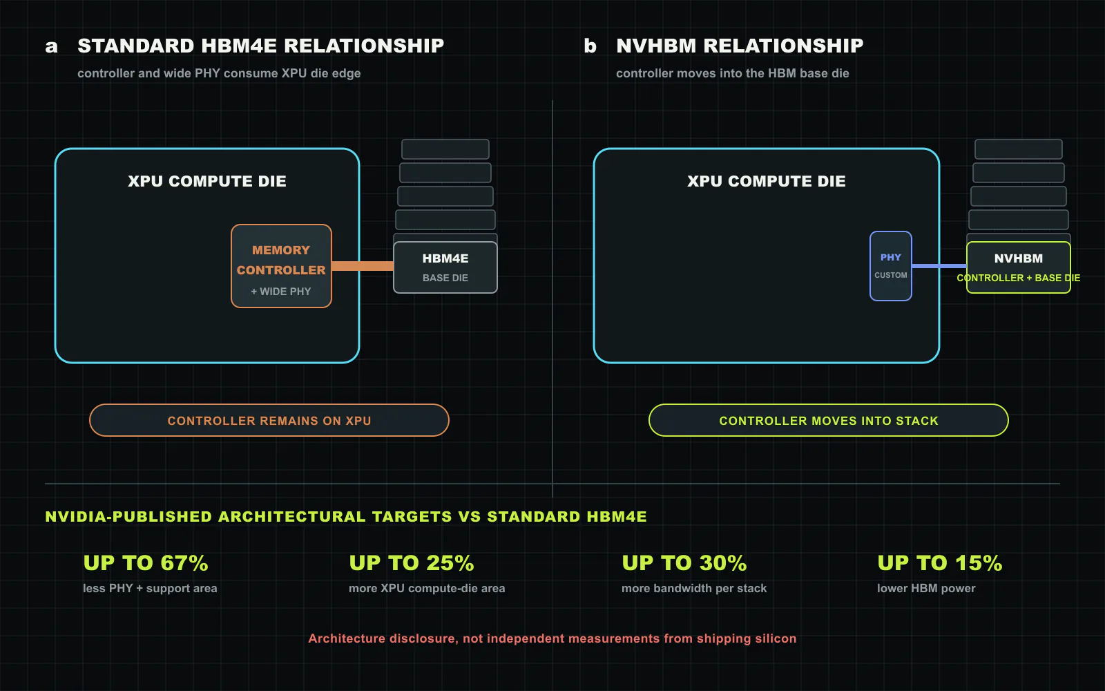
NVIDIA has proposed moving a part of the memory system that custom accelerator designers normally own. In NVHBM, NVIDIA’s custom memory controller resides in the HBM base die rather than the XPU compute die, while a custom physical interface connects the two. The company associates that arrangement with up to 30% more bandwidth per stack, up to 15% lower HBM power and up to 25% more XPU compute-die area than a standard HBM4E implementation[1][2]. These are not three independent speedups, and the last figure does not mean 25% higher application performance.
That distinction matters because the announcement combines three different products. NVHBM is a memory architecture, NVLink Fusion supplies chiplets and links that attach custom XPUs to NVIDIA’s rack-scale fabric, and MediaTek offers a prevalidated design and manufacturing route around them[3][5]. Amazon’s Annapurna Labs is the first named NVHBM collaborator, but the public statement describes work toward future Trainium designs rather than a shipping Trainium4 configuration[2][4]. The important development is therefore not a benchmark result. It is a change in who supplies the controller, who qualifies the HBM path and which parts of a custom XPU remain differentiated.
Why the controller occupies expensive silicon
HBM places stacked DRAM beside an accelerator on an interposer or other advanced package. The short, wide connection provides much more bandwidth than a board-level memory channel, but the DRAM stack is only one side of that connection. The XPU still needs logic that schedules requests, tracks state, applies ordering and reliability policy, and converts the controller’s transactions into electrical signals. In a conventional HBM relationship, the memory controller and a wide PHY sit along the compute die’s edge. They use leading-edge logic area even when their purpose is moving data rather than performing matrix or vector operations.
The edge location also has a geometric cost. A controller cannot be placed wherever empty standard cells happen to remain. Its PHY must line up with bumps and interposer routes, power must reach the interface, and timing closure must account for a large regular block at the die perimeter. The occupied area can fragment the remaining floorplan and constrain where network, cache and compute blocks fit. Thus, a reduction in interface area can be more valuable than the same number of square millimeters scattered through the die. NVIDIA has not published an XPU floorplan, so this possible placement benefit remains an engineering implication rather than a measured NVHBM result.
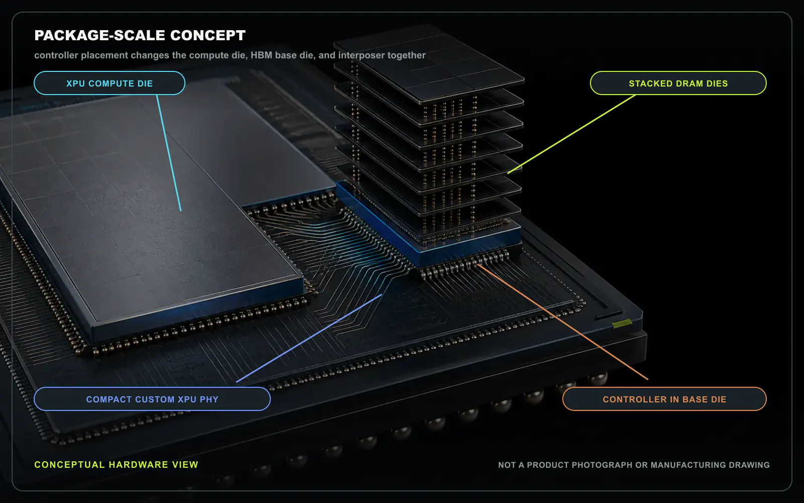
The base die under an HBM stack is already a logic-bearing layer. It terminates through-silicon vias from the DRAM dies and presents the external interface to the package. NVHBM gives that layer more responsibility by integrating NVIDIA’s custom memory controller there[1][2]. The stack therefore becomes more than a standardized memory endpoint. It contains logic that previously belonged to the accelerator design, and the compute die retains a smaller custom PHY for the connection.
The controller moves, but the whole memory system does not
The phrase “move the controller into HBM” can imply that the XPU simply deletes its memory subsystem. The disclosed architecture is narrower. NVIDIA states that its controller is integrated into a custom HBM base die and paired with a custom PHY; it does not disclose the register boundary, command protocol, cache-coherence behavior, error-reporting path or division of training logic between the XPU and the stack[1][3]. The XPU must still generate memory traffic, preserve the ordering required by its programming model and expose faults to firmware and fleet management. Some control state therefore remains on the compute side even if the DRAM controller itself changes layers.
Physical separation also remains. Requests still cross an interface, interposer routes and microbumps before reaching the base die, then travel vertically through the stack. NVHBM is not processing-in-memory and does not place tensor arithmetic beside the DRAM arrays. Its purpose is to redesign the attachment so that less interface area and power are spent on the compute die while the memory stack accepts more controller responsibility.
This arrangement creates a co-design problem across process technologies. The compute die is optimized for dense, high-speed logic. The HBM base die must balance logic, routing, TSV placement, thermal behavior and memory-vendor manufacturing flows. Moving controller logic can save expensive XPU area, but it can also enlarge or complicate the base die and make its yield, test coverage and repair strategy more important. NVIDIA has not published base-die area, process node, redundant resources or known-good-die procedure. Those omissions do not refute the idea, but they prevent a package-cost calculation.
Four percentages, four denominators
NVIDIA’s most specific claim is that the redesigned PHY and supporting circuitry use up to 67% less area than the company’s reference implementation of standard HBM4E[1]. That percentage concerns the interface block, not the entire XPU. A two-thirds reduction in one peripheral region cannot be applied directly to every die. The benefit depends on how many HBM stacks attach, how much edge each interface consumes, and whether the recovered regions can be assembled into placeable compute, SRAM or networking blocks.
The second figure is up to 25% more XPU compute-die area available for additional capabilities[1][2]. NVIDIA’s technical article is internally inconsistent here: its comparison table uses 25%, while a later paragraph says the reclaimed space provides up to a 30% increase in available main-die silicon. The corporate announcement repeats 25%. We therefore use 25% as the more consistently stated figure and preserve the discrepancy rather than averaging the two. Even then, “available area” is not the same as a smaller die, a 25% increase in arithmetic units or a 25% reduction in cost. A designer can spend that area on compute, cache, I/O, redundancy or guard bands, and each option changes performance and yield differently.
The third claim, up to 30% more memory bandwidth per stack than standard HBM4E, uses a bandwidth denominator[1]. NVIDIA has not published pin rate, bus width, stack capacity, read/write mix, access efficiency or sustained application bandwidth. A memory-bound kernel could benefit if the controller and PHY deliver the claimed increase under its access pattern. A compute-bound kernel will not. An application that is limited by collective communication, host I/O or scheduling may see no material change until those constraints are removed.
The fourth claim, up to 15% lower HBM power, concerns the memory subsystem rather than the full XPU, rack or facility[1][2]. NVIDIA illustrates the possible scale by stating that the saving could create headroom for as many as 15,000 additional 2,000 W XPUs in a 1 GW datacenter[1]. The public text does not expose the assumed HBM share of device power, utilization, cooling overhead, reserved capacity or power-delivery losses behind that projection. A facility planner should therefore retain the figure as a vendor scenario and request watts at the package input under a defined memory workload before converting it into deployable accelerator count.
NVIDIA also claims a combined 30% end-to-end performance increase per XPU from bandwidth, area and power improvements[1]. The three inputs cannot be multiplied mechanically: freed die area produces no throughput until a chip implements useful logic there, lower HBM power helps only if power or thermals constrain sustained operation, and bandwidth matters only during memory-limited phases. Without a named workload, baseline XPU, power limit and completed-work metric, the 30% result is an architectural projection rather than a benchmark.
Multi-vendor memory with one controller owner
NVIDIA says NVHBM will have a standard implementation offered by multiple memory providers[2]. This could remove a genuine burden from custom XPU programs. Qualifying an advanced HBM generation requires coordinated work across controller design, PHY, packaging, signal integrity, thermal behavior, test and supplier variation. A controller and base die validated with several suppliers can shorten that work and give a hyperscaler more than one manufacturing source without maintaining separate controller paths.
However, multi-vendor supply is not the same as an open memory interface. NVIDIA describes the controller as its own design and NVHBM as part of NVLink Fusion. Public material does not include an implementable interface specification, licensing terms, interchangeability guarantees or a process for qualifying a memory vendor outside the program[1][3]. The proposal horizontally opens the list of memory manufacturers while vertically concentrating the controller architecture and validation method. That can be a sensible trade for teams that value schedule and rack integration, but it should be priced as an ecosystem choice rather than a drop-in JEDEC component.
The commercial boundary matters during failure analysis. If a stack fails qualification, the cause could reside in DRAM, base-die controller logic, the custom PHY, interposer routing, package assembly or XPU firmware. A production contract must define who owns diagnosis, which telemetry crosses the interface and whether a stack from another qualified supplier can replace it without an XPU mask change. Until these details are published, “multiple providers” establishes an intention for supply resilience, not field interchangeability.
AWS proves interest, not product performance
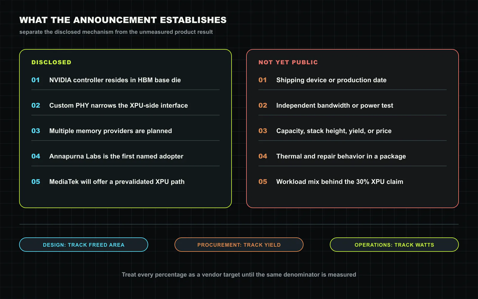
Amazon’s Annapurna Labs is the first named company working with NVIDIA on NVHBM. The joint AWS and NVIDIA release says the collaboration would give Trainium access to faster, more power-efficient memory and allow Trainium and NVIDIA GPUs to share a common rack-scale architecture through NVLink Fusion[4]. The wording is prospective. It does not state that Trainium4 tape-out contains NVHBM, list the number or capacity of stacks, or provide a delivery date and benchmark.
The partnership is still important because Annapurna Labs already owns a mature custom accelerator and cloud deployment stack. Its participation indicates that NVHBM addresses a real integration problem, not only NVIDIA’s internal GPU roadmap. Yet partner interest is not independent validation of the four percentages. AWS and NVIDIA issued the announcement jointly, and no Trainium system using NVHBM was available for measurement at publication time.
MediaTek’s August 31 announcement adds a second layer. MediaTek will offer NVLink Fusion as a foundation for customer XPUs, including the Fusion chiplet, NVLink-C2C and NVHBM, together with packaging, manufacturing and rack-level validation[5]. This route lets a customer concentrate on workload-specific compute logic while purchasing much of the surrounding system integration. It also means that memory, package and fabric decisions arrive as a coordinated platform. A buyer saves engineering schedule but accepts more preselected interfaces and suppliers.
This is why NVHBM belongs in a memory analysis rather than a simple partnership story. The base-die controller is the technical device that connects supplier qualification at the bottom of the stack to rack compatibility at the top. Its value is partly electrical, but its larger commercial function is to turn a custom XPU into a semi-custom platform component.
The evidence required before a design win
The first validation step is a matched package comparison. Fabricate otherwise comparable XPU test vehicles with standard HBM4E and NVHBM, then report total compute-die area, controller and PHY area, interposer area, package yield and usable frequency. The result should show whether the recovered edge region accepts useful compute or SRAM without creating new timing, power-delivery or routing constraints. Gross free area alone is insufficient.
The second step is a memory characterization with capacity and temperature attached. Sustained read, write and mixed bandwidth should be measured across access sizes and bank behavior, together with idle and loaded HBM power. Thermal tests must show the DRAM and base-die controller at steady state, since additional logic beneath the stack changes where heat is generated. Tail latency, corrected-error reporting and behavior after a degraded channel matter as much as peak bandwidth for production inference.
The third step is an application test that keeps the denominator stable. Compare completed training steps or SLO-valid inference tokens at the same model, precision, batch policy, package power and rack cooling limit. Record whether the workload was constrained by local HBM, compute, NVLink collectives, scale-out networking or host I/O before and after the change. Only a local-memory-limited phase can attribute its gain directly to NVHBM bandwidth.
Finally, procurement needs supply evidence: qualified memory vendors, compatible stack capacities, lead times, base-die ownership, test responsibility, licensing, field-failure procedure and substitution rules. A technology can meet its electrical targets and still be unattractive if the controller creates a single validation path or if the base die reduces yield enough to erase the saved compute area.
A memory architecture that sells integration
NVHBM’s most consequential move is not the headline percentage. It relocates the memory controller from a hyperscaler’s differentiated compute die into an NVIDIA-designed base die, then offers that memory through a rack-scale integration program. The customer may gain usable silicon, bandwidth, power headroom and a shorter qualification schedule. In return, NVIDIA participates in the accelerator even when the main compute die carries another company’s architecture.
That bargain can be valuable. Custom silicon teams routinely spend years and substantial engineering capacity on interfaces that do not differentiate their workloads. A validated memory path can redirect those resources toward arithmetic, cache, compiler and service behavior. However, the recovered schedule and silicon must be measured against controller dependence, package yield, multi-vendor substitutability and actual completed work per watt.
The right current conclusion is narrower than “25% more compute.” NVIDIA has disclosed a credible way to change where memory-control logic is built and who qualifies it. The next evidence must show that the freed area becomes useful circuitry, the lower interface power survives at package input, and several memory suppliers behave as one operational supply pool. Until then, NVHBM is a serious architectural proposal and an ecosystem strategy, not a shipping performance result.
Source and copyright notice
This article is an independent Silicon & Systems industry analysis prompted by TechTimes reporting and based primarily on NVIDIA’s technical disclosure, its NVLink Fusion architecture page, the joint AWS announcement, and the joint MediaTek announcement. Vendor projections are labeled as such and are not treated as measurements from shipping silicon. No source sentence, table, diagram, photograph or product rendering is reproduced. All figures were created for this article; the material plate is a conceptual illustration with deterministic labels, not a product photograph or manufacturing drawing. Source materials are © their respective publishers and companies, 2026.