AMD Helios should be evaluated as a rack design, not as 72 independent MI455X specifications. Four-GPU trays, 31 TB of HBM4, UALink over Ethernet and pluggable AI NIC choices define the service and communication boundaries that software sees. Peak MXFP4 and memory totals describe capacity; useful training or inference throughput still depends on collective efficiency, power, cooling and failure recovery.
The announcement changes a system boundary
A high-end accelerator can hold a larger model, but training and distributed inference slow down when the scale-up domain is difficult to repeat, cable or repair. Proprietary rack assemblies may optimize one generation while forcing customers to replace networking and management assumptions with every accelerator cycle. The obvious response is to compare AMD’s largest number with a competing device. That misses the architectural choice. The relevant boundary is where software state, memory ownership, communication and repair move together. A peak specification matters only after the deployment preserves that boundary under load.
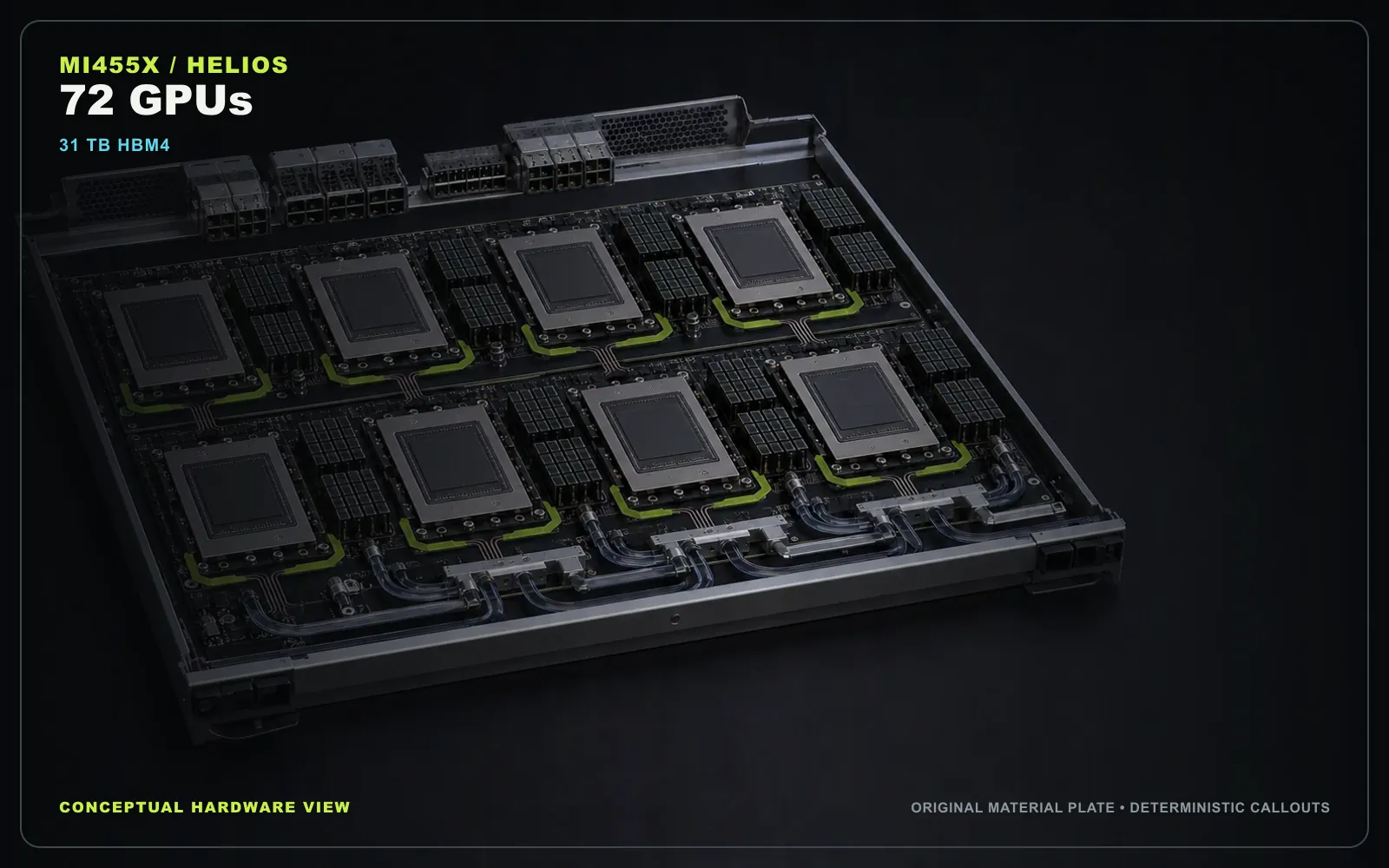
MI455X uses eight compute chiplets with 3D hybrid bonding and separate I/O dies. Each device carries 12 HBM4 stacks for 432 GB and 23.3 TB/s. Helios repeats four-GPU trays until 72 GPUs form an all-to-all, single-hop UALoE fabric. AMD lists either two PCIe 6 compatible NICs or three AMD AI NICs per enhanced accelerator module, separating scale-up connectivity from scale-out attachment choices. These values come from AMD’s public material and describe the announced configuration. They should not be read as independent measurements or as performance available to every workload.
Reading the specifications without mixing denominators
The disclosed anchors are 432 GB and 23.3 TB/s per GPU; 31 TB and 1.67 PB/s per rack; up to 2.9 EFLOP/s peak MXFP4. Each number answers a different question. Device capacity determines whether model or application state can remain local. Link and memory bandwidth set upper bounds before protocol, access pattern and contention. Core or arithmetic counts describe available machinery, while application completion depends on utilization and synchronization. Adding them together produces a visually impressive rack total but not a reproducible service result.
Company announcements are useful primary evidence for implementation facts because the supplier controls the design. They are weaker evidence for comparative economics because the supplier also selects the baseline, software and operating point. We therefore retain the announced values but label projections, supported maxima and vendor-run results. A neutral comparison would hold request mix, software maturity, facility power and availability targets constant.
The mechanism that is likely to persist
The four-GPU tray is the more important unit than the rack total. A repeatable tray gives manufacturing, cable reach, coolant routing and replacement a stable boundary, while UALoE lets a switch fabric extend that boundary to 72 GPUs. The procurement question is whether one failed module can be isolated without breaking the collective topology or forcing an entire 72-GPU job to restart.
This mechanism can outlast the first product generation because it identifies where coordination belongs. It also creates a new obligation. Telemetry has to expose queueing, memory pressure, link utilization, throttling and faults at the same granularity as the service boundary. Without those counters, an operator can observe a slow application but cannot distinguish silicon saturation from placement, communication or recovery overhead.
What the disclosure does not establish
AMD labels Helios a reference design shared with partners and expects volume deployments in the second half of 2026. The stated 2.9 EFLOP/s, 1.4 EFLOP/s and 1.67 PB/s are peak aggregate specifications, not application measurements. Public pages do not provide collective curves by message size, rack input power, coolant conditions, job completion rates or degraded-topology behavior.
Absence of those measurements is not evidence that the design fails. It defines the next acceptance test. Roadmap language should remain separate from shipping hardware; peak values should remain separate from sustained application rates; and a supplier’s comparison should remain separate from independent reproduction. This evidence discipline is particularly important in AI infrastructure because one missing rack component can change both performance and power denominators.
A practical qualification plan
A useful evaluation starts with three workloads rather than one synthetic peak. The first should maximize arithmetic with state that fits locally. The second should pressure memory capacity and bandwidth with realistic access skew. The third should cross the intended communication boundary using the message sizes and concurrency expected in production. All three should report completed work at p50, p95 and p99 latency rather than only average device utilization.
Power should be measured at the rack input and separated into compute, memory, networking, host, cooling and idle components. An operator should repeat the test after removing one replaceable module, one link and one network path. Time to isolate, remap and return to the service-level objective is often more valuable than the best healthy-system result. A design with a lower peak can deliver more useful capacity if it loses less work during maintenance.
Software qualification must record compiler and runtime versions, kernel coverage, model changes, fallbacks and time spent tuning. The test should distinguish software that already runs from software that needs product-specific reconstruction. It should also verify observability: counters need to explain where time and energy were spent, not merely show that a device was busy.
Procurement can then compare four totals: useful work per rack-hour, useful work per facility kilowatt-hour, capacity available during a component failure, and engineering time per new workload. Those denominators translate AMD’s architecture into an operating decision without discarding the genuine structural contribution.
The decision after Hot Chips
AMD’s announcement is important because it changes where a complete unit of compute can be built and managed. The durable question is whether the new boundary reduces movement and operational fragmentation after all supporting components are counted. Buyers should request the missing evidence at that exact boundary, while software teams should prototype placement and failure behavior before treating the largest specification as deployable capacity.
Integration economics beyond the headline device
The installed system has to reserve capacity for management, redundancy and maintenance. A nominally available core, link or memory channel may not be schedulable for a user job when it protects a failure domain or carries control traffic. Qualification should therefore publish both physical capacity and allocatable capacity under normal operation, during a component drain and after a failure. The same architecture can look efficient at peak load and expensive when a service objective requires spare paths.
Topology also changes software economics. A compiler may treat nearby memory or peers as a uniform resource, while the physical system contains several latency and bandwidth tiers. The runtime needs placement rules that match those tiers and must expose when it falls back to a longer path. Otherwise, an application update can silently alter communication and erase the benefit attributed to the new silicon. For AMD, the useful deliverable is not just a device API. It is a reproducible mapping from application state and collective operations to the physical hierarchy.
Lifecycle costs begin before deployment. Firmware signing, secure boot, isolation, error reporting, memory and network qualification, and existing orchestration integration all consume engineering time. They continue after launch as models, kernels and operating systems change. A supplier-controlled stack can optimize those layers together, but it can also make performance dependent on one release cadence. Buyers should request a supported-version matrix, rollback procedure and documented degraded mode rather than assuming that architectural compatibility guarantees operational compatibility.
Security and reliability should be tested at the new boundary. Shared memory, mixed instruction environments, modular accelerators and programmable transports create different questions, but the method is common: identify who owns an address, who can issue work, where errors are contained and which component can reset another. Fault injection should cover corrupted data, timeout, link loss and partial restart. The outcome is not only whether the system recovers, but also how much unrelated work is interrupted and whether state remains auditable.
Finally, utilization must be connected to delivered service. High device occupancy can coexist with poor completion when work waits in a network queue or is retried after a fault. Operators should correlate application traces with hardware counters and energy at the same timestamp. That correlation shows whether the new boundary removes movement or merely hides it inside another layer.
Source and copyright notice
This article is an independent Silicon & Systems editorial digest based on AMD’s official release and the cited primary material. We rewrote the architecture, specifications and limits in our own language and did not reproduce company slides, tables, diagrams or marketing images. The hardware plate and card motif were created for this article from rights-tracked, text-free source material; deterministic labels were added in code. Copyright in the cited source material remains with its respective owner (2026).