A 400 Gb/s optical lane is not obtained by making only the modulator faster. At approximately 200 GBaud PAM4, the package that connects the driver to the modulator becomes a radio-frequency circuit. A bond wire adds inductance, a dielectric trace adds capacitance and loss, and a height error changes the electrical path. Mitsubishi Electric’s Journal of Lightwave Technology paper is valuable because it follows this chain from the electro-absorption modulated laser (EML) device through a hybrid submount to a package concept that removes the bond wire[1].
The work targets the next step after 1.6 Tb/s DR8 optics. Eight lanes at 200 Gb/s produce 1.6 Tb/s; reusing the eight-lane arrangement at 400 Gb/s would produce a 3.2 Tb/s module. The authors associate that transition with GPU clusters, near-package optics (NPO), and co-packaged optics (CPO). Their prototypes do not yet deliver an error-qualified 400 Gb/s optical lane. Instead, the paper isolates three bottlenecks and measures a different artifact for each one. Keeping those artifacts separate is essential to reading the result correctly.
Why Mitsubishi stays with an EML
Several modulator platforms are candidates for 400 Gb/s per lane. Silicon photonics offers dense multi-lane integration. Thin-film lithium niobate and silicon-organic-hybrid devices can provide very high electro-optic bandwidth. Mitsubishi argues for an EML because an indium-phosphide laser and electro-absorption modulator can occupy a small footprint and operate with a drive swing below 1.0 Vpp. The quantum-confined Stark effect changes absorption efficiently, allowing a short modulator beside the laser.
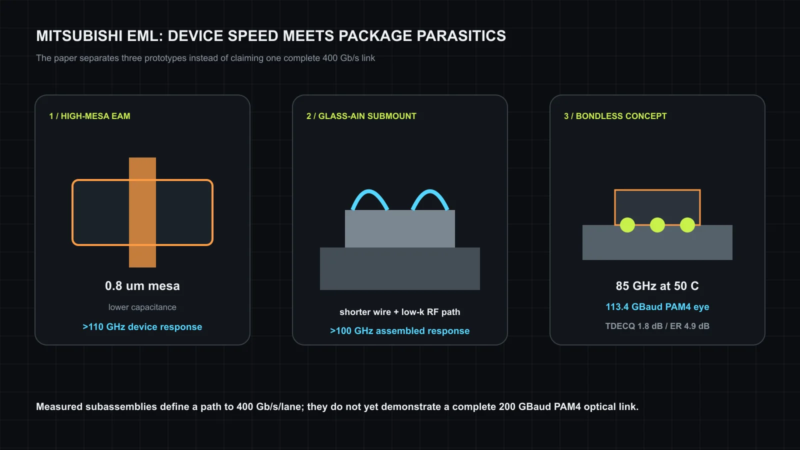
The same compactness creates a capacitance problem. The electro-absorption modulator (EAM) behaves as a small capacitor in the RF path. Reducing its mesa width lowers capacitance and raises the electrical bandwidth, but an excessively narrow mesa complicates fabrication, resistance, optical confinement, and thermal behavior. The paper studies high-mesa EAM widths of 1.1 and 0.8 micrometers. The 0.8-micrometer device reports a small-signal response beyond 110 GHz under the measured condition.
This is a device response, not a data-link result. A frequency-response curve shows how the optical modulation amplitude changes with an RF tone. A 400 Gb/s lane additionally needs a driver, impedance-controlled package, sufficient optical power, a receiver, equalization, FEC, and a PAM4 eye that meets the relevant transmitter-quality and BER limits. The narrow mesa removes one bottleneck while leaving the rest of the path visible.
A short bond wire still behaves like an inductor
The conventional assembly places the EML on an aluminum-nitride (AlN) submount and connects the EAM electrode with wire bonds. AlN provides mechanical stability and good thermal conduction, both important for a laser. At frequencies above 100 GHz, however, even a short first bond wire adds enough inductance to reshape the impedance. Simulations in the paper vary this wire length and show the modulation response degrading as it becomes longer. Around a 300-micrometer wire, the package rather than the EAM constrains the response.
Mitsubishi’s answer is a hybrid submount. AlN remains under the laser for heat spreading and mechanical support, while a quartz-glass RF substrate provides a lower-dielectric path near the modulator. Bringing the RF trace closer shortens the critical wire. The substrate can also carry matching and peaking structures that would be harder to realize on the conventional carrier.
Prototypes using the 1.1- and 0.8-micrometer EAMs on this glass-AlN structure report modulation bandwidth beyond 100 GHz. That result joins a fast device to a practical thermal carrier without surrendering the RF response to the package. It is the paper’s strongest evidence for a pluggable-module path because the assembly retains wire bonding and a recognizable submount process.
The authors note irregularities above 80 GHz in the measurement setup and estimate bandwidth while ignoring small dips attributed to the equipment. That is a reasonable disclosed procedure, but it makes the shape of the response and repeatability across samples as important as the single crossing point. Product qualification would need a distribution across devices, temperatures, aging, and assembly tolerances.
Removing the bond wire changes the assembly problem
NPO and CPO demand high edge density. Wire loops occupy lateral and vertical space, restrict pitch, and can interfere with neighboring optics and electrical traces. Mitsubishi therefore evaluates a junction-up concept in which the RF substrate sits over the EML and carries the signal through gold stud bumps rather than a long bond wire. Ground blocks flank the EML so that both signal and return connections can be reached from the top.
The mechanical details are not decorative. The EML and ground blocks are 0.2 mm wide with 50-micrometer gaps. Their arrangement can support a 500-micrometer optical pitch when repeated. Up to 10 micrometers of height mismatch may appear among the parts, so the prototype stacks two gold bumps on the lower EML and one on each ground block to align the contact plane. A quartz RF substrate then bonds directly over the assembly, with a termination resistor and peaking inductors integrated on the glass.
At an EML temperature of 50°C, this direct-connected prototype reaches 85 GHz of 3 dB bandwidth. The paper explains why it is slower than the hybrid wire-bonded case: a roughly 100-micrometer metal-filled via crosses quartz with relative permittivity around 3.8, and the double-stacked bumps add parasitic inductance. The authors suggest increasing via diameter as one route to improvement. Removing a bond wire therefore does not remove parasitics; it replaces a visible loop with vias, bumps, pads, and dielectric transitions that must be designed as a complete RF structure.
The PAM4 eye is 113.4 GBaud, not 200 GBaud
The bondless prototype produces a clear optical eye at 113.4 GBaud PAM4 with a 1.0 Vpp drive. The reported transmitter and dispersion eye closure for PAM4 (TDECQ) is 1.8 dB, and the extinction ratio is 4.9 dB. These numbers are meaningful because they move beyond a small-signal sweep and show data modulation through the package.
They are also well below the target symbol rate. PAM4 carries two bits per symbol, so 113.4 GBaud corresponds to 226.8 Gb/s before coding overhead. A 400 Gb/s lane needs close to 200 GBaud under the paper’s premise. The 85 GHz package bandwidth is consistent with the lower data rate and illustrates the remaining gap. The device and the hybrid wire-bonded assembly cross 100 GHz separately; the high-density bondless package demonstrates data at a lower bandwidth. No one prototype combines every best result.
The distinction guards against a common optics error: multiplying a component bandwidth by two and calling the result a shipping lane rate. PAM4 performance depends on noise, linearity, chirp, optical modulation amplitude, receiver bandwidth, equalization, and FEC. The paper establishes a route toward 400 Gb/s per lane, not a complete link at that rate.
What this means for GPU-cluster optics
Higher lane rate can reduce the number of lasers, modulators, detectors, fibers, and electrical lanes needed for a given module capacity. An eight-lane 3.2 Tb/s module could reuse DR8 fiber organization while doubling aggregate bandwidth over a 1.6 Tb/s generation. Fewer lanes can also relieve package-edge pressure around an accelerator or switch ASIC.
However, per-lane speed moves difficulty into analog margin. The driver and receiver must operate over a broader band, insertion loss becomes more expensive, and package discontinuities consume a larger fraction of the unit interval. CPO further exposes the optics to the thermal environment of a large switch or accelerator. Mitsubishi’s 50°C package result is relevant, but a product must characterize junction temperature, external laser conditions, neighboring-channel heating, and airflow over the full assembly.
Manufacturing yield may decide whether the high-density concept saves cost. The direct-connected assembly aligns an EML, two ground blocks, multiple stacked bumps, and a glass substrate. A 10-micrometer height variation is already large enough to require different bump stacks. An array multiplies those opportunities for open contact, impedance variation, or optical misalignment. Wafer-level or passive alignment can make the process economical only if test access identifies bad optical and electrical channels before they are attached to an expensive host package.
A useful paper because it does not hide the package
The enduring contribution is the separation of device, thermal carrier, and high-density integration. The 0.8-micrometer mesa shows that the EAM itself can cross the required frequency range. The glass-AlN submount shows that thermal and RF requirements can coexist above 100 GHz. The bump-connected package shows a plausible edge-density direction and quantifies the penalty that remains.
Those steps also explain why optics roadmaps cannot be evaluated from modulator bandwidth alone. At 400 Gb/s per lane, the package is a distributed RF network. Bond length, dielectric constant, via diameter, bump height, ground return, and temperature participate in the signal path. The best laboratory device is useful only when its package preserves enough of that response for the data eye.
The study extends Mitsubishi’s invited OFC 2025 paper[2] with additional measurements and analysis; we treat both as one linked research series rather than creating a duplicate conference post. The related SPIE Photonics West work[3] focuses on the same beyond-100-GHz submount. The peer-reviewed JLT article is the appropriate primary post because it combines the device and assembly evidence and openly marks what remains incomplete.
Source and attribution
This article is an independent editorial summary prepared by Silicon & Systems from the JLT record and the publicly available author version. The author manuscript states that it is licensed under CC BY 4.0. We restated facts and measurements in our own words and did not reproduce source text, tables, or figures. The figure and card were created for this article. The final Journal of Lightwave Technology version is (c) IEEE 2025/2026; citation data may differ between the early-access DOI and the Optica volume record.