AMD’s first exascale node did not use the integrated processor that its research program originally imagined. Frontier instead connected separate EPYC CPUs and Instinct GPUs because packaging, yield, and product schedules made a single large APU impractical. The ISCA 2024 paper is valuable because it explains how that abandoned idea returned as MI300A, and which physical constraints had to change before integration became rational[1].
One address space changes the node
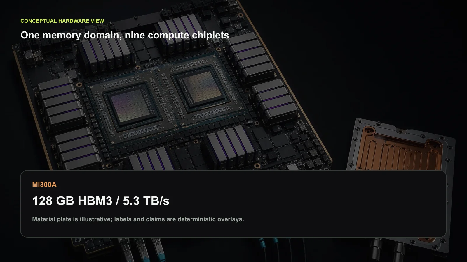
MI300A combines six CDNA 3 accelerator complex dies, three Zen 4 CPU dies with 24 cores, four base I/O dies, and eight HBM3 stacks. The 128 GB memory pool supplies about 5.3 TB/s and is coherent across CPU and GPU agents. A CPU can initialize a dataset in HBM and a GPU can consume it without copying the allocation through host DRAM. That is the architectural result. The package is not merely a smaller version of a discrete node; it changes which data movements software must schedule.
The paper also shows why simple reuse would have failed. A server I/O die carries DDR channels, external links, and topology assumptions that are useful for a socket but waste area and power inside an HBM-centered APU. AMD therefore distributed the base functions across four I/O dies and used short-reach links so that the package behaves as one fabric. Six GPU chiplets and three reused CPU chiplets are hybrid-bonded above those dies, while the HBM stacks sit beside them on an interposer.
Packaging becomes architecture
The integration budget is unusually large: about 146 billion transistors excluding HBM. Hybrid bonding provides dense vertical connections between compute and I/O dies, while 2.5D integration connects the four base dies and eight memory stacks. These technologies decide link energy, reachable bandwidth, repair options, and which chiplets can be reused. In this design, packaging is no longer a back-end implementation detail.
The trade-off is equally physical. A package that removes external data copies concentrates power and heat, increases assembly complexity, and makes known-good-die testing and yield management central to product economics. Unified memory also does not make every workload faster. Applications with little CPU-GPU sharing may benefit less, while workloads whose working set exceeds 128 GB still need a slower external tier.
The first exascale plan failed for useful reasons
AMD’s earlier exascale vision placed CPU and GPU compute close to one high-bandwidth memory system. Frontier ultimately used separate EPYC CPUs and Instinct accelerators. The change did not invalidate the architectural goal; it exposed that packaging capability, product schedules, risk, and yield were not yet aligned for an integrated part at the required scale.[1]
That history matters because MI300A is not presented as an obvious linear evolution. The design became feasible after reusable CPU and GPU chiplets, a purpose-built base die, high-density bonding, large interposers, and HBM integration matured together. Integration was chosen when it could remove a meaningful software and data-movement boundary without requiring one monolithic die.
The lesson for chiplet roadmaps is timing. A function should not move into a package merely because a diagram can connect it. The manufacturing stack, test strategy, reuse plan, software contract, and workload must all repay the assembly risk. Frontier’s discrete node and MI300A are two answers selected under different constraints.
The package has three physical layers of responsibility
Six accelerator compute dies and three CPU dies provide the reusable arithmetic. Four base I/O dies below them implement memory controllers, fabric, and package-level connectivity. Eight HBM3 stacks sit beside the logic on the interposer. This division avoids burdening the CPU chiplets with server-socket DDR and I/O functions that an HBM-centered APU does not need.
The base layer is not passive wiring. It determines how the four regions act as one addressable device and how traffic reaches HBM. Short-reach die-to-die links replace part of the board-level path, while dense vertical connections join compute to the base dies. The physical hierarchy therefore matches the protocol hierarchy: local vertical traffic, lateral package fabric, and HBM channels.
Using multiple small dies improves reuse and can improve wafer yield relative to one enormous logic die, but it adds assembly yield. A sellable package requires several known-good compute dies, four base dies, eight memory stacks, an interposer, and thousands of connections to work together. Test coverage and repair strategy become part of the architecture’s cost.
Coherent HBM changes ownership of data
In a discrete node, software commonly allocates host memory, copies a working set to accelerator memory, launches a kernel, and moves results back or manages two address spaces through a runtime. MI300A exposes 128 GB of HBM3 as one coherent pool for CPU and GPU agents. A CPU can prepare a structure where the GPU will use it, and both can exchange ownership without an explicit bulk copy through host DRAM.
Eliminating a copy does more than remove bandwidth. It removes synchronization and bookkeeping around allocation, transfer, and duplicate residency. Irregular CPU-GPU cooperation can operate on fine-grained shared structures that would be uneconomic to marshal repeatedly across a discrete link. Porting can also be simpler when the program no longer has to choose two physical memories for every object.
Coherence is not free uniformity. CPU and GPU caches, access granularity, locality, and contention still differ. A CPU-heavy phase can consume HBM bandwidth needed by the accelerator, and fine-grained sharing can generate coherence traffic. Software must place work and data with awareness of which agent dominates rather than assuming one address implies one latency.
Capacity and bandwidth are separate constraints
The pool provides about 5.3 TB/s of HBM bandwidth, far beyond conventional socket DRAM, but capacity is fixed at 128 GB in the reported design. Workloads that fit and share data between CPU and GPU can benefit strongly. A larger model, mesh, or data set still needs an external tier, node-to-node decomposition, or streaming policy.
Bandwidth is also not uniformly available to every access. Channel mapping, contention, locality to base dies, and the balance among six GPU dies and three CPU dies determine realized throughput. Peak HBM bandwidth is a package capability, not a guarantee that one kernel or a mixed CPU-GPU workload will sustain 5.3 TB/s.
The most useful evaluation therefore reports working-set size and movement eliminated in addition to kernel speed. A workload may run the same arithmetic rate yet finish sooner because it avoids copies. Another may see little change because data stays on the GPU for its entire lifetime. Integration is selected by the boundary it removes, not by HBM bandwidth alone.
Hybrid bonding shifts the energy budget
Dense vertical bonding permits many short connections between compute and base dies. Compared with long package traces or board links, each transferred bit can use less energy and occupy less edge perimeter. That makes it practical to separate compute from I/O without forcing all communication through a narrow chiplet interface.
The benefit must be evaluated against manufacturing complexity. Bond pitch, alignment, wafer or die preparation, thermal stress, and inspection affect yield. A defect in a connection may disable a large assembled module even when all component dies passed wafer test. Known-good-die screening and package-level diagnostics need to cover the high-density interface.
The approximately 146 billion transistors excluding HBM describe the integration scale, not a performance metric. Some transistors implement reusable compute, while others provide fabric, memory control, redundancy, and physical interfaces. The package is valuable when this supporting structure enables more useful work per node than the discrete components it replaces.
Thermal design follows the stack
Stacking compute above active base dies shortens wires but creates vertical heat paths. CPU and GPU phases can concentrate power in different regions, while HBM has its own temperature and reliability limits. Cooling must remove heat through the package without allowing one hot chiplet to throttle neighbors or memory.
Power delivery faces a similar hierarchy. Rapid GPU current changes, CPU boost behavior, and HBM traffic share package and board constraints. Voltage regulation and package planes must maintain integrity across mixed workloads. An integrated APU can reduce I/O energy yet concentrate the remaining load into a denser module.
For operators, sustained application clocks and facility conditions matter more than brief peak specifications. A workload that alternates CPU preparation and GPU computation may create a different thermal pattern from one that runs both agents concurrently. Procurement should use measured node power, cooling, and throttling under representative applications.
Software must expose the removed boundary
Hardware coherence creates an option; runtimes and programming models determine whether applications use it. Allocators need to place shared objects in the HBM pool, compilers need to preserve locality, and profilers need to show which agent caused bandwidth or coherence stalls. Legacy code that always copies into a GPU-owned buffer can run without capturing the architectural benefit.
Unified memory can also tempt developers to ignore movement until performance becomes unpredictable. Tools should distinguish page placement, migration, cache behavior, and explicit ownership transitions even when pointers are valid on both agents. The best software makes the common shared path simple while keeping physical movement observable.
Libraries and communication stacks need a node-level view. MPI and GPU-aware runtimes should know when a buffer is already coherent and avoid staging. Checkpoint and I/O systems can use CPU cores to prepare or compress data in place. These are system effects that a standalone GPU kernel benchmark will not measure.
Which workloads should gain most
Applications with frequent CPU-GPU handoff, irregular control, shared metadata, or fine-grained tasking have the clearest reason to use MI300A’s memory contract. Scientific simulations can let CPU code manage data structures that GPU kernels update. Graph and adaptive workloads can avoid repeatedly packaging irregular frontiers for a discrete transfer.
GPU-dominant dense computation whose data enters HBM once and remains there may benefit less from CPU integration. If the CPU is lightly used, its silicon and power provide limited value compared with a GPU-only package. Conversely, CPU-heavy workloads may prefer larger DDR capacity even if HBM is faster.
This makes MI300A a node architecture rather than a universal accelerator replacement. The correct comparison includes CPU sockets, external accelerator links, duplicated memory capacity, board power, and software movement. Comparing only GPU peak FLOPS would ignore the boundary the product was designed to remove.
Package economics determine scaling
Chiplets let AMD reuse CPU and GPU designs across products and avoid fabricating every function on the same process. The base dies can be optimized for I/O and connectivity, while compute uses a denser node. This improves portfolio flexibility and amortizes design cost.
Assembly, interposer area, HBM supply, bonding capacity, and test time add costs that wafer yield alone does not capture. A multi-die package may be economically superior even if its assembly yield is lower, provided reuse and smaller logic dies offset the loss. Repairable or partially enabled configurations can further change the equation, though the article should not assume capabilities the product does not disclose.
Buyers see the result through availability, price, and serviceability. A failed HBM stack or bonded interface may require replacing the entire module. Platform design therefore needs telemetry that localizes errors and procurement models that include module sparing, not only silicon throughput.
What future packages should disclose
Useful comparisons need the number and role of dies, memory capacity and sustained bandwidth, coherent agents, link topology, power boundary, and workloads that eliminate copies. Vendors should separate die-level yield claims from assembled-module availability and explain supported memory-reliability features.
Software evidence should include porting effort, data transferred before and after integration, CPU and GPU utilization, coherence overhead, and working-set limits. Thermal evidence should show sustained mixed-agent operation. These disclosures allow readers to judge whether an integrated package changes the system or merely places familiar parts under one lid.
The limit of the paper’s evidence
The paper explains design history and architecture; it does not provide a universal performance ranking against every discrete CPU-GPU node. Product documentation supplies specifications, while application outcomes depend on software and cooling. The benefit of 128 GB coherent HBM cannot be extrapolated to working sets that exceed it.
Its strongest evidence is causal. The design removes unused socket I/O, places a fabric under reusable compute chiplets, connects them densely, and presents HBM coherently. That sequence links package technology to a software-visible boundary and gives future chiplet systems a clearer standard than die count.
The next validation step is an application-level movement audit: bytes copied or staged, coherent traffic, CPU and GPU occupancy, HBM contention, node power, and time to solution on matched integrated and discrete nodes. That evidence would quantify the software boundary that the package removes.
What we take from it
MI300A demonstrates that heterogeneity becomes most useful when the memory contract is designed with the compute, not when separate devices are merely placed closer together. Its lasting lesson is the sequence of decisions: remove unused server I/O, shorten the fabric, make HBM coherent, and only then stack reusable compute chiplets. Future accelerator packages will be judged by the software-visible boundaries they eliminate, not by chiplet count alone.
Source and attribution
This article is an independent editorial summary written in our own words. No sentences, figures, or tables from the paper are reproduced. The figure was created for this article from reported facts. The public author manuscript states that copyright is held by the authors and publication rights are licensed to ACM; the proceedings version is © 2024 the owner/authors.