Chip compute scales roughly with area, while conventional I/O enters through the perimeter. Lightmatter frames this mismatch as the package shoreline problem: a larger collection of compute chiplets creates more demand for communication than its outer edge can supply. Passage M1000 replaces a passive interposer with a 3D photonic network that spans a 4,000 mm² silicon complex[1].
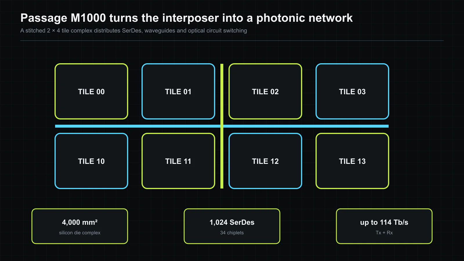
The platform stitches eight photonic tiles in a 2 by 4 arrangement. Up to 34 customer chiplets attach above the network through standard package processes, while 1,024 SerDes connect electrical endpoints to optical transmitters and receivers. Lightmatter states aggregate transmit-plus-receive bandwidth of up to 114 Tb/s and 256 fibers. The direction sum matters: 114 Tb/s is not 114 Tb/s simultaneously in one direction.
The architectural question is not whether a photonic interposer can expose a large lane total. It is whether making the interposer an active network increases delivered application bandwidth after routing contention, tuning power, power delivery, and assembly yield are included. This review uses that system boundary to distinguish platform specifications from evidence a populated AI package would still need to provide.
Microrings make the vertical stack possible
A photonic interposer needs conversion circuits small enough to sit under many electrical endpoints. Lightmatter uses microring modulators and receivers, reporting about 15 µm ring diameter and 0.006 mm² for a transmitter-plus-receiver circuit with an inductorless driver and analog front end. The measured examples include 56 Gb/s NRZ links, while 112 Gb/s PAM4 is also enabled in the platform[1].
Microrings combine modulation and wavelength multiplexing in a compact structure, but resonance shifts with temperature and process variation. Lightmatter reports a feedback-controlled operating range from 0°C to 105°C. The control loop, heater power and external laser are therefore part of the link, even when they do not appear in the area of one optical endpoint.
The interposer routes around faults
Each tile contains horizontal optical buses, cross-reticle waveguides and an optical circuit switch. The switch can select alternate fiber paths, so attachment redundancy becomes a routing resource rather than a spare connector. Electrical metal stitching also links neighboring tiles. This combination makes the interposer a two-layer network: optics carries long, high-bandwidth paths while metal handles local adjacency and control.
The platform must also deliver power and remove heat for the chiplets above it. Lightmatter shows a 369 mm² thermal test chip at 1.47 W/mm² and states that Passage through-silicon vias support more than 2.5 A/mm²[1]. These tests address the concern that a photonic layer under compute could obstruct power delivery. They are test-vehicle results, not a thermal specification for every 34-chiplet customer assembly.
What the M1000 number means
The specification table lists 4,000 mm² of silicon, 34 chiplets, 1,024 SerDes, 256 fibers and up to 114 Tb/s. These dimensions shift comparison away from one optical engine. The product is closer to an optical backplane manufactured with semiconductor processes. Lightmatter also presents future examples of 200 Tb/s XPU and 400 Tb/s switch connectivity, but those are platform projections rather than measured M1000 applications.
The most important limit is evidence level. The deck includes measured optical links, SerDes eyes, microring behavior, power-delivery test structures and tile details. It does not disclose a complete customer AI system benchmark, assembly yield across the full 4,000 mm² complex or field reliability. The platform claim is technically detailed, but commercial scale still needs customer deployment data.
The package becomes a network domain
Passage M1000 changes where switching occurs. Conventional packages connect fixed point-to-point electrical links and leave routing to external switches. An optical interposer can reconfigure paths inside the package and carry them directly to fiber. This may reduce the number of electrical boundaries between accelerators, but it also puts network control, photonic calibration and package manufacturing into one product.
That integration is the opportunity and the risk. If it yields, the interposer removes shoreline as the dominant I/O constraint and gives chiplet systems a fabric proportional to area. If calibration or assembly does not scale, a large shared photonic layer becomes a common failure and cost domain. The next decisive evidence will therefore be a shipped multi-chip system, not a larger aggregate bandwidth number.
The interposer becomes an active network substrate
A conventional silicon interposer primarily carries electrical wires between compute and memory chiplets. Passage adds a photonic routing layer and optical interfaces, so the substrate participates in communication rather than only providing geometry. Compute dies attach electrically over short local distances, while longer package-to-package paths can leave through fiber[1]. This division aims to reserve copper for the reach where it remains efficient.
An active interposer also concentrates dependencies. A fault in a passive wire may affect one link; a failure in shared photonic control, laser distribution or switching can affect several attached dies. The package architecture needs fault domains and bypass paths that match the expensive compute resources above it. Known-good-interposer testing becomes important because the value of the assembled compute dies can far exceed the substrate.
The 3D integration path has to manage micro-bump density, optical couplers, power delivery and mechanical flatness at once. Adding a photonic layer cannot consume the keep-out area needed for high-current power connections. The interposer must also route fibers without blocking cooling hardware or increasing assembly stress. These geometric constraints are part of the bandwidth result because they determine how many lanes can be built and serviced.
Tile arithmetic is not application bandwidth
The M1000 material describes a tiled organization whose aggregate bandwidth is obtained from repeated electrical and optical interfaces[1]. Tiling offers a path to a large fabric because the same block can be verified and composed. However, raw lane totals do not state how traffic is distributed, how many endpoints communicate simultaneously or how much capacity is lost to protocol and topology.
If several compute chiplets send to the same destination, internal links or the optical egress can become the limit before the sum of all lanes is reached. Conversely, balanced nearest-neighbor traffic may use a larger fraction of the local capacity. Useful evaluation therefore reports a traffic matrix and delivered bandwidth, not only the sum of physical ports. Collective communication should include all-reduce, all-to-all and failure cases because each stresses the fabric differently.
Latency also has several components. A local die-to-interposer transfer may be short, while an optical path includes modulation, propagation, switching and detection. Circuit establishment or reconfiguration can add another term if the topology uses optical switching. Applications with large bulk transfers can amortize setup; fine-grained synchronization may expose every stage.
Microrings trade density for control
Passage uses silicon photonic elements including microring-based functions. Rings are compact and can place many wavelength-selective devices in a limited area. Their resonance shifts with fabrication and temperature, so control loops must tune the devices to the intended wavelengths. The power and area of heaters, monitors and controllers belong in the interposer budget.
Tuning becomes a fleet problem when thousands of rings operate near hot accelerators. Calibration at manufacturing time is insufficient if workload temperature changes the operating point. Fast control can follow variation but may add noise and power; slow control can allow transient link margin loss. Telemetry should expose tuning range and residual margin so software can identify a degrading optical path before errors rise.
Wavelength-division multiplexing increases fiber bandwidth by placing several carriers on one waveguide. More wavelengths also tighten the requirements for laser stability, filter spacing and crosstalk. A channel-count projection must show that all wavelengths operate simultaneously across temperature, not only that one device can tune through the range.
Power delivery competes with signal density
AI packages draw large current at low voltage. The interposer and package need many low-resistance power paths, decoupling capacitors and voltage regulation while also carrying dense electrical and optical I/O. Allocating edge and substrate area to fibers does not reduce the current that must reach the compute dies. In some layouts, power delivery rather than signaling can set the number and position of attached chiplets.
Thermal design has the same competition. Photonics benefits from a controlled temperature, while compute dies create steep and changing hot spots. A cold plate optimized for the accelerators can constrain fiber routing or place pressure on optical structures. Moving lasers off package can remove one heat source but requires optical distribution and connector loss.
Energy-per-bit claims must include this shared infrastructure. Electrical SerDes, photonic modulation, detection, tuning, laser wall power, retiming and fabric control all contribute. Idle power is relevant because training traffic is phase-dependent; a fabric provisioned for peak collective bandwidth can spend time waiting during computation. Power gating or wavelength shutdown can help only if wake-up latency does not delay the next collective.
Optical circuit switching adds scheduling semantics
A reconfigurable photonic fabric can connect endpoints with low data-path energy once a circuit is established. The cost moves into choosing and configuring the circuit. If demand changes faster than the switch, traffic waits or falls back to a less direct path. The scheduler needs information about upcoming collectives, which creates an interface between the model runtime and network control.
Predictable training steps are an opportunity. Repeated collective patterns can be scheduled ahead of time, and circuits can be reused over many iterations. Mixture-of-Experts and inference traffic are less regular, making static schedules less effective. A hybrid design may reserve optical circuits for large predictable transfers while packet paths absorb bursts and control traffic.
Failure recovery must reconfigure both the optical path and the collective plan. A lost wavelength or fiber reduces capacity in a way that may be asymmetric across ranks. The runtime should avoid turning the slowest surviving path into a global straggler. Recovery time and degraded-mode bandwidth are as important as healthy peak bandwidth for long training jobs.
Manufacturing evidence will decide the platform
Hot Chips establishes the intended architecture, the active interposer concept and the scale of the M1000 integration. The remaining evidence spans manufacturing and system operation. It should include interposer yield, attached-die yield after assembly, fiber coupling distributions, simultaneous multi-wavelength error rates and thermal cycling. Repair or redundancy strategy should state how many lane failures can be tolerated without discarding the module.
System tests should drive a populated package and multiple packages through an actual optical topology. Delivered application bandwidth, tail latency, wall power and training-step time should be compared with a contemporary electrical baseline at the same reach and oversubscription. The comparison needs to count any electrical switches or retimers removed by the optical design and every laser or optical switch added.
Lightmatter’s central proposition is that the interposer can become the scalable network boundary of an AI package. This is more consequential than replacing one cable because it changes where chiplets attach and where traffic is switched. The concept is technically coherent. Its adoption will depend on whether active-interposer yield, thermal control, power delivery and fabric scheduling remain manageable when the impressive lane count is populated with expensive compute dies.
Source and copyright notice
This article is an independent editorial summary of Lightmatter’s official Hot Chips 2025 presentation. We preserved the directionality and evidence boundaries of the vendor figures and restated the architecture in our own words. No source slide, micrograph, chart or floorplan is reproduced. The explanatory figure was created specifically for this article. The presentation is (c) Lightmatter 2025, all rights reserved.