Co-packaged optics is often evaluated at the wrong moment. A photonic chiplet is characterized before package assembly, its coupling loss is low, and the lane reaches the target data rate. Production begins after that measurement. The die is placed, underfilled and exposed to solder reflow; the substrate bends; an array of fibers must remain aligned; temperature and humidity then act on every adhesive and interface. A few micrometers of motion can turn an optical margin into a failed lane.
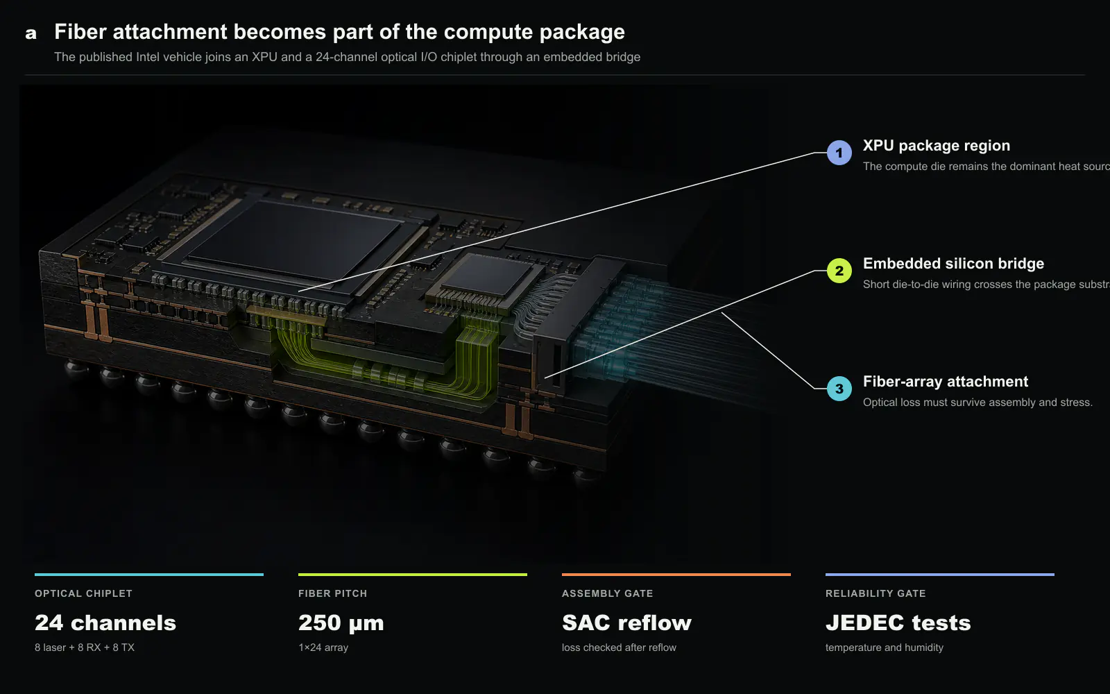
Intel’s ECTC 2025 paper addresses this manufacturing boundary. The test vehicle places an XPU and a fiber-connected optical I/O chiplet in one package and links the dies through Embedded Multi-die Interconnect Bridge (EMIB). The optical chiplet exposes 24 channels, organized as eight laser paths, eight receive paths and eight transmit paths. A 1×24 fiber array at 250 µm pitch is routed to a 2×12 MT-style interface[1][3]. The study follows insertion loss through assembly and then applies environmental and mechanical stress.
This is not a switch bandwidth record. The paper does not claim that the vehicle trains a large model or moves a stated number of terabits in an application. Its value is different: it treats fiber attach and package reliability as part of CPO architecture. Intel reports low, stable insertion loss after SAC solder reflow and no significant optical degradation in the summarized JEDEC temperature cycling, unbiased highly accelerated stress, high-temperature storage and mechanical tests[1][3]. The conclusion is a process result, not a fleet benchmark.
The optical interface is also a mechanical interface
An electrical bump can tolerate some geometrical error because current still flows through a deformed conductive contact. Optical coupling is less forgiving. A fiber or waveguide must overlap a mode whose dimensions are measured in micrometers. Lateral shift, vertical separation, angular error and adhesive shrinkage can each increase insertion loss. The loss can also be polarization-dependent or different across fibers in the same array.
That sensitivity changes how package tolerances should be allocated. The substrate supplier, optical chiplet, fiber-array vendor, adhesive and assembly line all contribute to the final alignment. A single nominal loss number cannot identify which process owns the margin. Production needs distributions by channel, package location, assembly lot and stress condition. The relevant question is not whether one optical path couples; it is whether enough of 24 paths stay inside the budget after the complete flow.
The 250 µm pitch makes the physical scale visible. Twenty-four fibers occupy millimeters of package edge before strain relief and connector mechanics are included. This edge must coexist with electrical escape routing, power delivery, cooling hardware and board keep-outs. CPO reduces high-speed electrical reach, but it replaces some of that board routing with a fiber-management problem at the package boundary.
The 2×12 interface also introduces a service boundary. A manufacturable system must decide whether the fiber assembly is permanent, pluggable or replaceable with the package. Each choice changes loss, cost and repair. A permanent connection can minimize interfaces but turns fiber damage into package replacement. A connector helps assembly and service, yet adds alignment surfaces and contamination risk.
EMIB solves one distance and creates a joint process
EMIB places a small silicon bridge inside an organic substrate so adjacent dies can communicate over short, dense wiring without using a full silicon interposer. For CPO, that allows the XPU and optical I/O chiplet to use separate process technologies while keeping the high-speed electrical path short. The compute die can prioritize transistors and memory interfaces; the optical die can prioritize waveguides, modulators, detectors and analog circuits.
This partition avoids monolithic yield coupling, but it does not make the dies independent. Bump pitch, bridge routing, clock architecture and power integrity must be closed across the boundary. The optical chiplet sits in the thermal and mechanical field created by the XPU and substrate. Assembly order also matters: a fiber attach performed early must survive later reflow, while a late attach must fit within the alignment and access left by the completed package.
The Intel paper’s emphasis on assembly is therefore architectural. The electrical bridge, optical coupling and package process have to form one qualified flow. Optimizing only the die-to-die channel can produce a package that cannot be built economically; optimizing only optical coupling can leave the electrical edge too long or too power-hungry.
The bridge also localizes one failure mode. A defective optical chiplet may be screened before final assembly if known-good-die tests cover electrical and optical functions. However, the fiber interface is not fully exercised until it is attached, and the final bridge path may not be represented by wafer probing. Test coverage must follow the assembly sequence rather than assume that die-level pass results multiply into package yield.
Reflow is a decisive checkpoint, not a formality
SAC reflow raises the package to the temperature needed to form lead-free solder joints. Materials with different coefficients of thermal expansion move by different amounts during heating and cooling. Organic substrate, silicon, glass fiber, metal and adhesive do not expand together. Warpage can shift the optical interface temporarily or permanently, while adhesive properties can change after thermal exposure.
Reporting insertion loss before and after reflow therefore closes an important manufacturing question. Stable loss suggests that the attachment and material stack retain alignment through this step. It does not by itself establish lifetime. Reflow is a short event, whereas deployed hardware experiences years of thermal cycling, vibration and humidity. Still, failure at reflow would make later reliability irrelevant, so it is the first hard gate.
The useful production metric is a paired distribution. Each channel should be measured before reflow, after reflow and after stress, allowing the shift to be separated from initial assembly variation. Mean loss can stay stable while a tail of channels fails. CPO economics are sensitive to that tail because a package with many optical lanes can be rejected by one or a small number of outliers unless redundancy is designed in.
Rework complicates the contract. Reheating a package or replacing a nearby component may expose the fiber attach to another thermal cycle. A process qualified for one reflow does not automatically tolerate multiple excursions. Manufacturing documentation should state allowable reflow count, peak temperature, time above liquidus and handling load on the fiber assembly.
Reliability tests must map to optical failure physics
Temperature cycling tests expansion mismatch and fatigue across repeated hot-cold transitions. High-temperature storage accelerates material changes that can shift adhesion or optical properties. Unbiased highly accelerated stress combines temperature and humidity to expose moisture-related degradation without electrical bias. Mechanical shock and vibration probe connector, fiber and attach robustness. Intel’s summarized results report no significant optical degradation across the applied test set[1][3].
Passing these tests is necessary, but the reported condition and sample count determine how much confidence to assign. A qualification statement should include duration, temperature range, humidity, mechanical spectrum, package population and acceptance threshold. The paper establishes that the integration route can be subjected to recognized package reliability methods; it does not provide field-return statistics for a shipping CPO product.
Optical monitoring should also distinguish reversible drift from permanent damage. Temperature can move the coupling point during a measurement and then recover, while adhesive creep or delamination can create a lasting shift. Measuring only at room temperature after stress can miss hot-state loss that matters in operation. A production platform needs both in-situ operating curves and post-stress inspection.
The XPU changes these physics because it is a strong, nonuniform heat source. Reliability coupons without active compute power cannot fully represent the gradient seen beside a large accelerator. Future evidence should combine electrical workload, cooling contact pressure and live optical margin. CPO is valuable precisely because the optics are close to the hot die, so that proximity cannot be excluded from qualification.
Twenty-four channels make yield a system variable
The channel organization is more informative than a single aggregate bandwidth claim. Eight laser paths distribute light, eight receive paths bring optical data toward the XPU, and eight transmit paths carry data outward. A failure in a laser path can affect multiple dependent signals depending on the internal split. Transmit and receive loss budgets may differ because modulators, detectors and couplers contribute different penalties.
This means lane availability cannot be summarized by average insertion loss. Architects need a dependency map from laser input through optical components to electrical lanes. If one fiber or laser path disables several channels, redundancy should be placed before that shared point. If failures are independent, spare individual lanes may be sufficient. The physical organization determines the cheapest recovery scheme.
Test time is part of the cost. Measuring 24 optical paths across temperature and manufacturing stages can dominate final test if alignment or wavelength sweeps are slow. Built-in monitors, loopback and calibrated optical taps may increase die area but reduce package test time. A high-volume claim should therefore include throughput and false-reject behavior, not only whether a laboratory setup can measure every path.
Known-good optical die is more difficult than known-good digital die because some defects appear only after fiber coupling. Wafer-level optical probes can screen modulators and detectors, but the final mode conversion and array geometry are assembly-specific. The paper’s flow is a step toward closing this gap because it keeps optical performance visible through package processing.
What the paper proves and what remains open
The work proves that a fiber-based optical I/O chiplet can be integrated beside an XPU with EMIB and carried through a credible package assembly and reliability program. It shows that insertion loss need not collapse after solder reflow and that the summarized environmental and mechanical stresses did not produce significant degradation[1][3]. This is stronger evidence of manufacturability than a pre-package eye diagram alone.
It does not report application traffic, full port power or a comparative cost against pluggable optics. It also does not establish field lifetime across every cooling and connector configuration. Aggregate lane rate, bit-error performance under active XPU heat, laser efficiency and repair strategy remain necessary to judge a product.
The missing evidence should be added without losing the process view. A complete study would report channel-by-channel loss distributions, package warpage, thermal maps, bit-error rate and energy before and after stress. It would state how many failed lanes can be tolerated and how they are remapped. It would also measure optical performance while the XPU executes a representative workload.
The system insight: CPO moves the qualification boundary
Pluggable optics isolates the transceiver behind a connector and a board trace. CPO removes much of that electrical distance, but it also moves the optical interface into the compute package’s manufacturing and reliability domain. The gain is not free. Optical alignment becomes subject to the same reflow, warpage, cooling pressure and service decisions as the XPU.
Intel’s paper is valuable because it evaluates this trade at the point where products often fail: assembly. EMIB provides the short electrical path, while the 24-channel fiber system exposes the optical and mechanical path. Neither can be qualified alone. The practical CPO metric is usable optical bandwidth after assembly stress per manufactured package, including the yield and test cost required to obtain it.
For buyers and system architects, this changes the questions posed to a CPO vendor. Peak Tb/s is not enough. Ask for per-channel loss distributions before and after reflow, active-temperature margin, stress sample count, connector or fiber replacement policy and the surviving lane rule. A design that answers those questions may deliver less impressive laboratory density but more deployed bandwidth. That is the difference between a photonic demonstration and a package technology.
A package-level acceptance specification
The paper points toward a concrete incoming and final-test specification. At optical-die receipt, measure modulator, detector and monitor functions that can be reached before assembly. After die attach and bridge connection, verify electrical loopback and power integrity. After fiber attach, record every channel’s insertion loss and polarization sensitivity. Repeat the same channel map after reflow and qualification stress, preserving the identity of each lane.
Acceptance should be based on usable lane count and loss margin, not only population average. A product may allow one spare transmit and receive lane, but a failed shared laser path may consume several lanes at once. The specification must therefore include dependency groups as well as individual channels. It should also distinguish repairable assembly defects from latent material changes that require package rejection.
This sequence gives operations a baseline. Field telemetry can compare received power, laser setting and temperature with the post-assembly channel map. A slow loss increase can then be detected before error correction is exhausted. Without that baseline, the system can remain logically healthy while spending more laser power and losing failover margin. The reliability paper closes the manufacturing side of this loop; future product data should connect it to fleet monitoring.
Source and copyright notice
This article is an independent Silicon & Systems editorial analysis based on Intel’s ECTC paper, the official ECTC program and a public IEEE EPS technical presentation. We restate the reported assembly and reliability scope in our own words and do not reproduce source photographs, cross-sections, plots or tables. The hardware plate was created specifically for this article and is not an Intel product rendering. The source paper copyright is (c) IEEE 2025. See doi:10.1109/ECTC51687.2025.00012.