The revealing number in Google’s eighth-generation TPU announcement is not 12.6 FP4 PFLOPS. It is two. Google has taken one accelerator generation and built two system architectures around it: TPU 8t for large-scale training and embedding-heavy work, and TPU 8i for post-training, high-concurrency reasoning and serving[1]. The distinction reaches beyond an execution unit. Memory capacity, on-chip SRAM, specialized engines, inter-chip topology, pod size, host CPUs and the scale-out network all change with the phase of the AI lifecycle.
That split acknowledges a problem accelerator comparisons often hide. Training can trade individual-step latency for high sustained utilization across a regular collective schedule. Autoregressive serving cannot. Every generated token may wait for state reads, reductions, expert routing and the slowest dependency in a chain. A topology that is efficient when thousands of chips exchange predictable gradients can impose too many hops when any token may route to any expert. Conversely, a compact low-diameter serving pod may leave performance on the table when a months-long training run needs more aggregate compute and memory.
Google’s public material provides enough detail to understand the design direction, but not enough to rank a finished cloud service. The stated gains compare both TPU 8 systems with the seventh-generation Ironwood, and Google still describes customer availability as forthcoming[2][3]. We therefore separate architectural facts from vendor projections and use the missing evidence to define a procurement test.
One generation stops pretending that one fabric fits every phase
TPU 8t and TPU 8i share the eighth-generation software environment and Arm-based Axion CPU heads, but their resource ratios point in opposite directions. TPU 8t exposes 216 GB of HBM, 128 MB of Vmem, 6,528 GB/s of HBM bandwidth and 12.6 peak FP4 PFLOPS per chip. TPU 8i exposes 288 GB of HBM, 384 MB of Vmem, 8,601 GB/s of HBM bandwidth and 10.1 peak FP4 PFLOPS[1]. The serving part has 20% less advertised FP4 compute, yet 33% more HBM capacity, about 32% more HBM bandwidth and 3× the on-chip memory.
Those ratios are more informative than the product suffixes. TPU 8t spends the generation budget on arithmetic throughput and a larger coherent training domain. TPU 8i spends more of it on keeping state near the cores and reducing the time of synchronization. Neither chip is incapable of the other workload. The point is that the expensive surrounding resources are sized for different critical paths.
The host choice matters for the same reason. Google integrates Axion CPU heads into both systems to handle data preparation and orchestration without starving the TPU. This is not a claim that a host bottleneck disappears under every input pipeline. It does show that Google treats preprocessing and control as part of accelerator utilization rather than an external server problem. An MXU waiting for tokenization, data transformation or a host-mediated transfer cannot recover that lost time by having a higher peak FLOPS number.
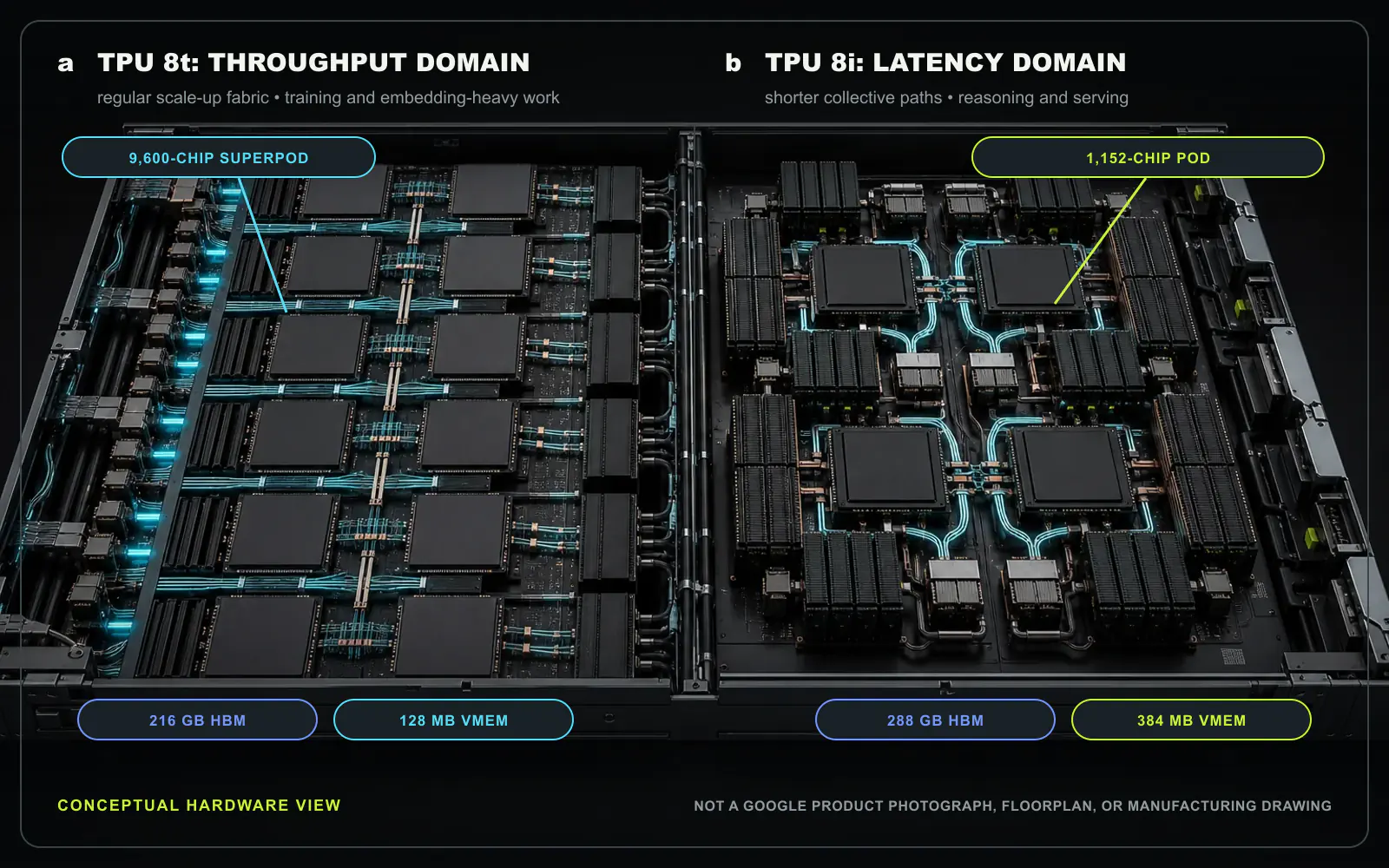
TPU 8t widens the training domain
TPU 8t retains a 3D-torus inter-chip topology and scales one superpod to 9,600 chips. Google associates that system with 121 exaflops and 2 PB of shared HBM, then uses Pathways and JAX to describe training clusters above one million chips[2]. These are different boundaries: a superpod is the scale-up domain, Virgo connects much larger collections at the data-center layer, and software coordinates work across sites. Treating the million-chip figure as one flat all-to-all machine would erase the hierarchy that makes it possible.
Inside the chip, TPU 8t attacks three forms of lost utilization. SparseCore handles irregular embedding lookups and selected data-dependent collectives instead of making the matrix engine process mostly empty work. More balanced VPU scaling allows quantization, softmax and layer normalization to overlap more effectively with MXU work. Native FP4 halves the bits moved per low-precision value relative to FP8 and doubles the stated MXU throughput, subject to a model and training recipe preserving acceptable accuracy[1]. Each change aims to keep provisioned arithmetic active rather than merely increasing its theoretical ceiling.
The I/O path expands with the compute domain. Google states that TPU 8t doubles ICI scale-up bandwidth over Ironwood and that Virgo provides up to 4× the raw scale-out data-center network bandwidth. Virgo is described as a two-layer, non-blocking, multi-plane fabric that can link more than 134,000 TPU 8t chips with 47 Pb/s of bisection bandwidth[1]. The important architectural choice is the collapsed hierarchy: higher-radix switches reduce network layers, while independent planes limit the fault and control scope. The published figures still need workload-level validation because raw bisection bandwidth does not disclose congestion, retransmission, collective scheduling or application efficiency.
Storage is also placed on the training critical path. TPUDirect RDMA bypasses host CPU and DRAM for transfers between HBM and the network interface. TPUDirect Storage provides a direct path between the TPU and Managed Lustre. Google reports doubled transfer bandwidth for the direct-storage path and up to 10× faster storage access than Ironwood training when it is paired with Managed Lustre 10T[1]. The claim is configuration-specific, not a universal storage multiplier. Its larger meaning is sound: a training system that can checkpoint, reload and feed multimodal data at line rate preserves expensive compute time during events that ordinary accelerator benchmarks omit.
TPU 8i spends silicon on waiting
TPU 8i changes the optimization target from long-run utilization to the latency of dependent steps. Its 384 MB of Vmem is three times the previous generation and three times TPU 8t’s capacity. Google says the additional SRAM can hold a larger KV cache on silicon, reducing core idle time during long-context decoding[1]. It cannot hold the complete KV state of every large model and concurrency level; placement, quantization and batching still determine what remains local. The relevant advantage is avoiding some HBM accesses and synchronization at the point where each token waits for the result.
The Collectives Acceleration Engine (CAE) replaces four SparseCores from the Ironwood core dies with one engine on the chiplet die alongside two Tensor Core dies. It accelerates reductions and synchronization used by autoregressive decoding and chain-of-thought processing. Google reports up to a 5× reduction in on-chip collective latency[1]. That is a specialized latency result, not a 5× end-to-end inference claim. If memory fetch, expert communication, host scheduling or software serialization dominates a workload, the observable benefit will be smaller.
Boardfly extends the same latency priority beyond one package. A TPU 8i tray forms a four-chip building block. Eight boards are connected into a localized group, and 36 groups connect through optical circuit switches. Google describes a pod with up to 1,152 installed chips and up to 1,024 active chips. For a 1,024-chip comparison, the maximum path falls from 16 hops in an 8 × 8 × 16 torus to seven hops in Boardfly, a 56% smaller network diameter. The company reports up to 50% lower latency on communication-intensive workloads[1]. Installed capacity, active capacity, topological diameter and application latency are four different quantities and should remain separate.
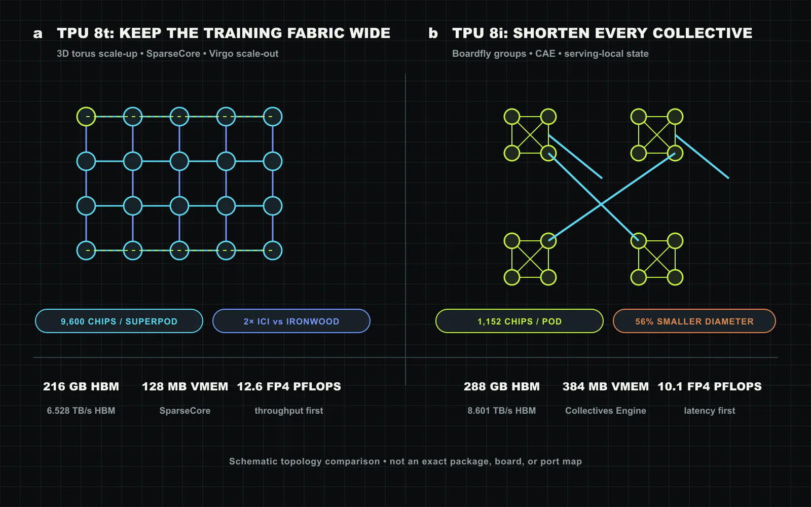
The network split follows the communication pattern
Dense training generally performs scheduled collectives over tensors whose placement is known before execution. A torus can exploit regular neighbor traffic, distribute links across dimensions and grow into a large domain without requiring every node to have direct reachability. Its cost is diameter. Traffic that must cross several dimensions consumes hops, and a global all-to-all pattern can expose that cost.
Reasoning and mixture-of-experts serving produce a different pattern. Token routes depend on model state and gating decisions, while the next step waits for current communication to finish. A high-radix hierarchy uses more direct links and switching resources to reduce the worst path. That can lower collective and tail latency, but it also concentrates design complexity in cabling, optical circuit switching, routing and reconfiguration. Boardfly should therefore be evaluated not only at steady state but while links fail, groups are drained and optical paths are changed.
The two designs also imply different scheduling questions. TPU 8t needs the compiler and runtime to place large meshes, overlap compute with collectives and preserve useful work when a slice of a very large cluster is unavailable. TPU 8i needs the runtime to keep latency-sensitive groups compact, place KV state close to execution and avoid creating a software queue that nullifies a seven-hop fabric. Hardware diameter is only valuable if placement and admission control keep the request inside the intended domain.
Software must preserve specialization without exposing every wire
Google presents JAX, Pallas, Mosaic, XLA, Pathways, Keras, vLLM and a preview of native PyTorch support as one stack spanning both systems[1]. Pallas and Mosaic give kernel authors hardware-aware control over SparseCore and CAE features. XLA is intended to hide Boardfly placement and CAE synchronization from ordinary model code. Native PyTorch support aims to reduce the framework barrier for teams that do not want to rewrite a model around JAX.
That combination creates a useful tension. An abstraction should keep application code portable, but performance depends on exposing enough topology and memory behavior to the compiler. A model may execute correctly on both TPU 8 systems while reaching very different utilization because its sharding, collective shape or custom kernels match only one. “Same code runs” is therefore an entry criterion, not proof of equivalent efficiency.
A production evaluation should measure migration as a distribution, not a demonstration. Teams need the fraction of operators that compile without change, time spent replacing unsupported kernels, numerical differences after FP4 conversion, recompilation behavior across shapes, debugging quality and the operational cost of maintaining a TPU-specific path. Native PyTorch being in preview is relevant because correctness coverage and performance tuning mature at different rates. Software portability can be a major advantage, but it must be included in total cost rather than inferred from a framework logo.
Google’s gains are generation comparisons, not a market ranking
Google reports up to 2.7× better training performance per dollar for TPU 8t than Ironwood, up to 80% better inference performance per dollar for TPU 8i, and up to 2× better performance per watt for both chips[1]. These values establish the intended direction and indicate that specialization is expected to pay economically. They do not yet disclose the price, workload suite, latency targets, rack power, cooling boundary, utilization, availability reservation or error bars needed to compare with an external GPU system.
The reference generation also matters. Ironwood is Google’s seventh-generation TPU, so the result measures Google’s own progress under its selected configurations. It does not show whether TPU 8t beats a Vera Rubin cluster on time to train, or whether TPU 8i beats a competing inference ASIC at the same model, quality, token latency and wall power. Such comparisons may eventually be favorable, but the public evidence does not establish them.
Availability is another evidence boundary. Google’s April announcement says both systems will become available to cloud customers, and the product page still directs prospective users to an interest form[2][3]. A launch claim and a generally orderable service are not the same state. Capacity by region, quota lead time, committed-use pricing, maintenance behavior and support terms determine whether an architectural advantage can be used on a production schedule.
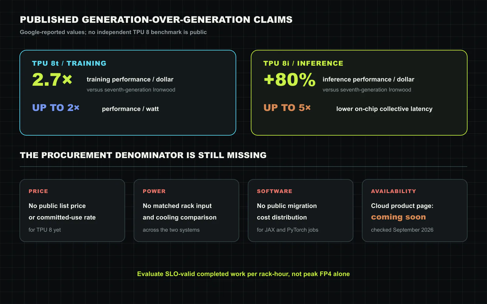
A procurement test should follow completed work
TPU 8t should be tested with a real training graph, dataset and checkpoint policy. The acceptance metric is time to a fixed model-quality target, including compilation, data ingestion, checkpoint writes, restart after a failed worker and periods when the global batch cannot use every provisioned chip. Report accelerators allocated, accelerators productive and wall energy separately. This exposes whether the 9,600-chip domain, Direct Storage and Virgo preserve useful work outside the steady-state training loop.
TPU 8i needs a serving matrix rather than one throughput score. Sweep input length, output length, batch size, concurrency, MoE routing skew and KV-cache pressure. Hold model quality and precision policy constant, then report time to first token, inter-token latency, p50, p95 and p99 completion latency, accepted requests per second and wall energy. Repeat after a group or link failure. A design that improves median collective latency but creates a long reconfiguration tail may not satisfy an interactive SLO.
Both systems need a matched cost boundary. Include TPU consumption, Axion hosts, scale-out network, storage, reservation discounts, idle headroom, cooling and the engineering time required to port and operate the workload. Divide that total by training runs that reach the target quality or inference requests that finish within the SLO. Peak FP4 per dollar is useful for capacity planning only after the application demonstrates that it can turn those operations into completed work.
The enduring change is system-level specialization
TPU 8 is important because Google no longer asks one pod topology to cover the whole AI lifecycle. TPU 8t treats arithmetic, embeddings, storage and a very large fabric as one throughput machine. TPU 8i trades some peak FP4 for more HBM, 3× the Vmem, a collective engine and a network with fewer worst-case hops. The chip table reflects the split, but topology and data placement create it.
The same design question applies beyond Google’s cloud. As training, reinforcement learning and long-running agent services diverge, an accelerator vendor can preserve one universal platform, divide products by phase, or expose composable resources that change with the workload. The winning option will not be the one with the most specialized block diagrams. It will be the one whose software maps real jobs to those resources without moving state, losing availability or multiplying operational paths.
For now, Google’s architecture gives operators a clear hypothesis to test: use a wide regular hierarchy when aggregate training throughput dominates, and use a compact low-diameter hierarchy when each dependent collective governs user-visible latency. TPU 8t and 8i make that hypothesis concrete. Price, wall power, failure behavior, migration effort and independent application results will decide its value.
Sources and copyright notice
This independent editorial digest is based on the publicly accessible Google Cloud architecture deep dive, the Google Cloud Next 2026 infrastructure announcement, the current TPU product page and the public Hot Chips 2026 program listing[1][2][3][4]. The access-controlled Hot Chips slides and session video were not used as technical evidence. No source figure is reproduced. The conceptual hardware plate, topology schematic, evidence chart and card motif were created for this article from our own composition and code. Source text and product information remain copyright their respective owners, including Google LLC and Hot Chips 2026.