Co-packaged optics (CPO) is usually introduced as a distance argument. Copper traces become lossy as lane rate rises, so the optical engine moves closer to the switch or accelerator. That description is correct but incomplete. Moving the conversion point does not automatically remove the electrical cost. The modulator still needs voltage swing, bandwidth and linearity, while its insertion loss must be paid by the laser. A large traveling-wave structure can also consume the package edge that CPO is supposed to preserve.
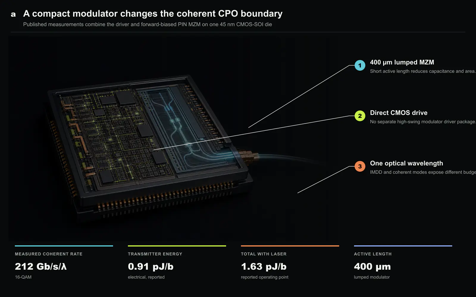
The ISSCC 2026 paper from UC Berkeley, MediaTek and Ayar Labs attacks this local boundary rather than the rack-level network. Its 45 nm CMOS-SOI transmitter directly drives a 400 µm forward-biased PIN Mach-Zehnder modulator (MZM). The measured operating points are 106 Gb/s PAM4 for intensity modulation and 212 Gb/s 16-QAM for coherent transmission on one O-band wavelength[1][2]. The coherent result is important because it combines phase and amplitude information without requiring a long standalone modulator beside the electronics.
The headline does not mean that a complete 212 Gb/s CPO port consumes 0.91 pJ/b. That number is the reported transmitter electrical energy at the coherent operating point. The public technical summary gives 1.63 pJ/b after laser power is included[2]. Receiver, clocking, control, redundancy and package-level losses remain outside that number. The correct conclusion is therefore narrower: a compact carrier-injection MZM can move the transmitter portion of coherent CPO into a competitive energy and area range.
Why the modulator length changes the package
A conventional traveling-wave MZM treats the electrode as a transmission line. The optical wave and the electrical wave must remain sufficiently matched along a millimeter-scale path. That approach can deliver bandwidth, but it brings electrode loss, termination power, routing area and a physical structure that is difficult to repeat many times around a large compute package. The driver also sees a load whose impedance and packaging must be controlled at radio frequencies.
The reported transmitter instead uses a lumped 400 µm device. Electrically, a lumped modulator looks more like a capacitance than a distributed line over its useful bandwidth. Shortening it reduces active area and can reduce the charge that the driver must move. The public summary reports about five times better modulator area efficiency than a traveling-wave implementation on the same die[2]. That comparison matters for CPO because shoreline length is limited: every optical lane competes with power delivery, memory interfaces, die-to-die links, test structures and fiber attachment.
Carrier injection brings a different constraint. Forward bias injects carriers into silicon and changes its refractive index efficiently, but carrier lifetime can limit speed and create nonlinear behavior. A coherent transmitter also needs controlled amplitude and phase, so the driver and modulator cannot be optimized independently. The paper’s contribution is not simply choosing a smaller device. It uses monolithic electronic-photonic integration to shape a short nonlinear device into a useful high-rate transmitter.
That integration changes which interface has to be closed. A separately packaged modulator asks the electrical driver to cross bumps and interconnect before reaching the optical device. A monolithic implementation removes that boundary but ties the photonic process, transistor performance and thermal behavior to one die. The saved parasitic load is real; the combined manufacturing constraint is real as well.
Two operating points answer two different questions
The 106 Gb/s PAM4 result uses intensity-modulation direct detection (IMDD). It is the simpler receiver contract: optical power represents amplitude levels, and the receiver detects intensity. The public summary reports 93 mW and 0.88 pJ/b for that transmitter operating point[2]. It demonstrates that the short injected-carrier device can support a practical four-level signal without a coherent receiver.
The 212 Gb/s result uses 16-QAM coherent modulation. Four bits are carried per symbol by controlling two quadratures. Coherent detection can extract phase as well as amplitude, but it also requires optical hybrids, local-oscillator handling, balanced detection and digital signal processing at the receiver. The transmitter consumes 194 mW, corresponding to the reported 0.91 pJ/b[1][2]. Similar electrical energy per bit at twice the bit rate is the notable result, not evidence that the whole link is equally simple.
These modes should not be treated as direct substitutes. IMDD may win when reach, density and receiver simplicity dominate. Coherent signaling can win when spectral efficiency, optical loss tolerance or wavelength count limits the system. A CPO architect must compare both ends of the link at the same bit-error target, coding overhead, laser allocation and reach. Quoting transmitter energy alone can reverse the decision if the coherent receiver is ignored.
The O-band choice also sets a condition. Silicon waveguides and short-reach fiber can benefit from operation near 1.3 µm, including relatively low chromatic dispersion in standard single-mode fiber. However, laser efficiency, coupling loss and the surrounding ecosystem can differ from C-band coherent telecom components. The paper establishes an O-band transmitter operating point, not a universal optimum across every CPO link.
Laser power belongs inside the boundary
Optical energy cannot be evaluated only at the electrical driver. A modulator with lower electrical swing may introduce more optical loss, forcing the laser to launch additional power. The public Berkeley summary states 1.63 pJ/b when laser power is included and reports a 1.5× improvement over a standalone lumped MZM and a 1.45× improvement over a conventional traveling-wave MZM on the same die[2]. Those comparisons are more useful than the 0.91 pJ/b value by itself because they expose the trade between voltage and photons.
Still, the laser boundary needs careful reading. Wall-plug efficiency converts electrical input into optical output, and distribution loss reduces the power that reaches each modulator. A shared external laser may gain thermal isolation and serviceability but pays splitter, connector and routing losses. An integrated laser can shorten the optical path but introduces heat and yield coupling. The phrase “laser included” is meaningful only when efficiency and delivered optical power are defined at the same points.
The reported total should therefore be used as a transmitter comparison point, not a rack budget. A deployed CPO port adds receiver photodiodes and amplifiers, clock recovery or coherent DSP, forward error correction, control processors and spare lanes. Package and fiber attach can change optical loss after the die is characterized. The paper moves one important line; it does not erase the surrounding system.
Monolithic integration trades parasitics for yield coupling
Putting electronics and photonics on the same CMOS-SOI die eliminates chip-to-chip electrical bumps between the driver and modulator. That reduces capacitance, wiring uncertainty and package assembly count. It also gives the circuit designer direct knowledge of the photonic load. These benefits are strongest for a direct-drive architecture because there is little room for an intermediate electrical interface.
The cost is shared yield. A defect in the photonic region can discard working electronics, while a transistor defect can discard a good optical lane. Process steps must serve low-loss waveguides, junction profiles and fast logic together. CPO products usually need many lanes, so the relevant yield is not one working transmitter but the probability that enough lanes pass optical and electrical tests across a large die or chiplet.
Redundancy can soften this multiplication. A tile may include spare wavelengths, spare lanes or remapping around failures. That choice consumes area and laser budget, and it needs test access before expensive package assembly. The 400 µm active length helps because a smaller repeated cell creates less defect opportunity and shoreline pressure. However, the paper does not publish a multi-lane production yield distribution.
Thermal variation creates another coupling. Forward-biased junction behavior changes with temperature, and the optical phase of an MZM drifts. A transmitter placed beside a switch ASIC may see gradients and workload transients that do not appear in a laboratory die measurement. Bias control can track those changes, but the monitor, heater or tuning loop also consumes energy. A credible package claim therefore needs measured operation across temperature with neighboring compute power applied.
Linearity is the coherent constraint
PAM4 needs separated amplitude levels, whereas 16-QAM needs accurate points in two dimensions. Driver distortion, modulator nonlinearity, phase imbalance and noise rotate or spread the constellation. Carrier injection is efficient precisely because it changes carrier density strongly; that same response is not naturally linear over an arbitrary swing.
Electronic-photonic co-design can use that nonlinearity rather than pretending it is absent. Driver segmentation, bias selection, digital predistortion and receiver equalization can divide the correction work. The proper objective is minimum link energy at a target error vector magnitude and post-FEC bit-error rate. Maximizing the standalone modulator bandwidth may spend more driver and laser energy than a slightly bandwidth-limited device paired with modest equalization.
This is also why the 212 Gb/s demonstration should be read as a joint circuit-photonic result. The modulator alone did not produce a valid 16-QAM signal, and the driver alone cannot overcome an unsuitable optical transfer function. ISSCC is the appropriate venue for that boundary because the result depends on measured circuits, device behavior and energy rather than only a network architecture.
What would make it a CPO building block
The next proof should repeat the transmitter across a useful lane count. A product-facing experiment would report lane-to-lane optical loss, phase balance, bias range and energy distributions, not only a representative lane. It would also show aggregate bandwidth under a shared laser and clocking architecture. The difference between 212 Gb/s on one wavelength and tens of terabits per package is manufacturing statistics.
Package evidence is equally important. Fiber coupling must maintain loss through reflow or another attach flow, and the transmitter must operate beside a realistic thermal load. The electrical result should include control, clocking and any equalization needed across process, voltage and temperature. Receiver energy must be reported at the same target reach and coding condition.
Reliability will be specific to the injected-carrier device. Repeated bias and temperature cycles can change junction leakage, phase response and calibration range. Laser safety margins must cover aging without making the day-one energy number irrelevant. None of these missing items invalidates the ISSCC result. They define the work between a circuit milestone and an optical I/O product.
The system insight: spend complexity where it removes a boundary
The strongest lesson is not that coherent modulation should replace every IMDD lane. It is that CPO gains depend on which boundary is removed. Moving an optical engine next to a switch while retaining a large driver-to-modulator interface leaves significant electrical and area cost in the package. Monolithic direct drive removes that interface and lets the modulator be shaped around the circuit.
That decision should be evaluated against alternatives such as tightly bonded electronic and photonic chiplets. Chiplets can separate process yields and allow a photonic process optimized for loss. Monolithic integration can minimize parasitics and repeated package wiring. The 400 µm transmitter strengthens the monolithic side of that comparison, particularly where shoreline density is the limiting resource.
The measured 212 Gb/s 16-QAM lane is therefore a boundary experiment. It shows that a forward-biased, lumped silicon modulator can be compact, fast and energy competitive when its electronics are designed with it. It does not show a finished CPO fabric. For system architects, the right follow-up question is precise: after adding laser distribution, receiver, control, redundancy, fiber attach and thermal margin, does the removed electrical interface still produce the lowest energy and highest usable bandwidth per package edge? That answer will determine whether this circuit becomes a lane in an AI cluster rather than only an ISSCC record.
Four normalized quantities for procurement
The result also suggests a practical comparison format for future optical engines. First, report usable Gb/s per millimeter of package shoreline after spare lanes and fiber mechanics are included. Second, report transmitter and complete-link pJ/b at the same post-FEC error target, with laser wall-plug efficiency stated. Third, report the loss and energy distribution across lanes and temperature rather than only the best channel. Fourth, report which control and equalization functions are counted on the optical tile, host or receiver.
These quantities prevent two common errors. A compact die can look dense while its fiber connector consumes the saved edge, and a low transmitter number can look efficient while the receiver or laser pays the difference. They also make monolithic and chiplet implementations comparable without assuming that one integration style is always superior. Monolithic integration should win where removed parasitics and shoreline dominate; chiplets should win where process specialization, test and replaceable yield dominate.
For this ISSCC transmitter, the measured lane rate, active length and transmitter energy are strong entries in that table. Multi-lane shoreline, full-link power and production distributions are not yet available. Keeping the blank cells visible is more informative than filling them with estimates, because those blanks define the next experiments required before a system buyer can compare it with a packaged optical engine.
Source and copyright notice
This article is an independent Silicon & Systems editorial analysis based on the ISSCC paper metadata, the official ISSCC 2026 program and UC Berkeley’s public technical summary. We distinguish measured transmitter results from our system-level implications and do not reproduce the source paper’s prose, die photograph, plots or tables. The hardware plate was created specifically for this article and is not a product rendering. The source paper copyright is (c) IEEE 2026. See the original publication at doi:10.1109/ISSCC49663.2026.11409273.