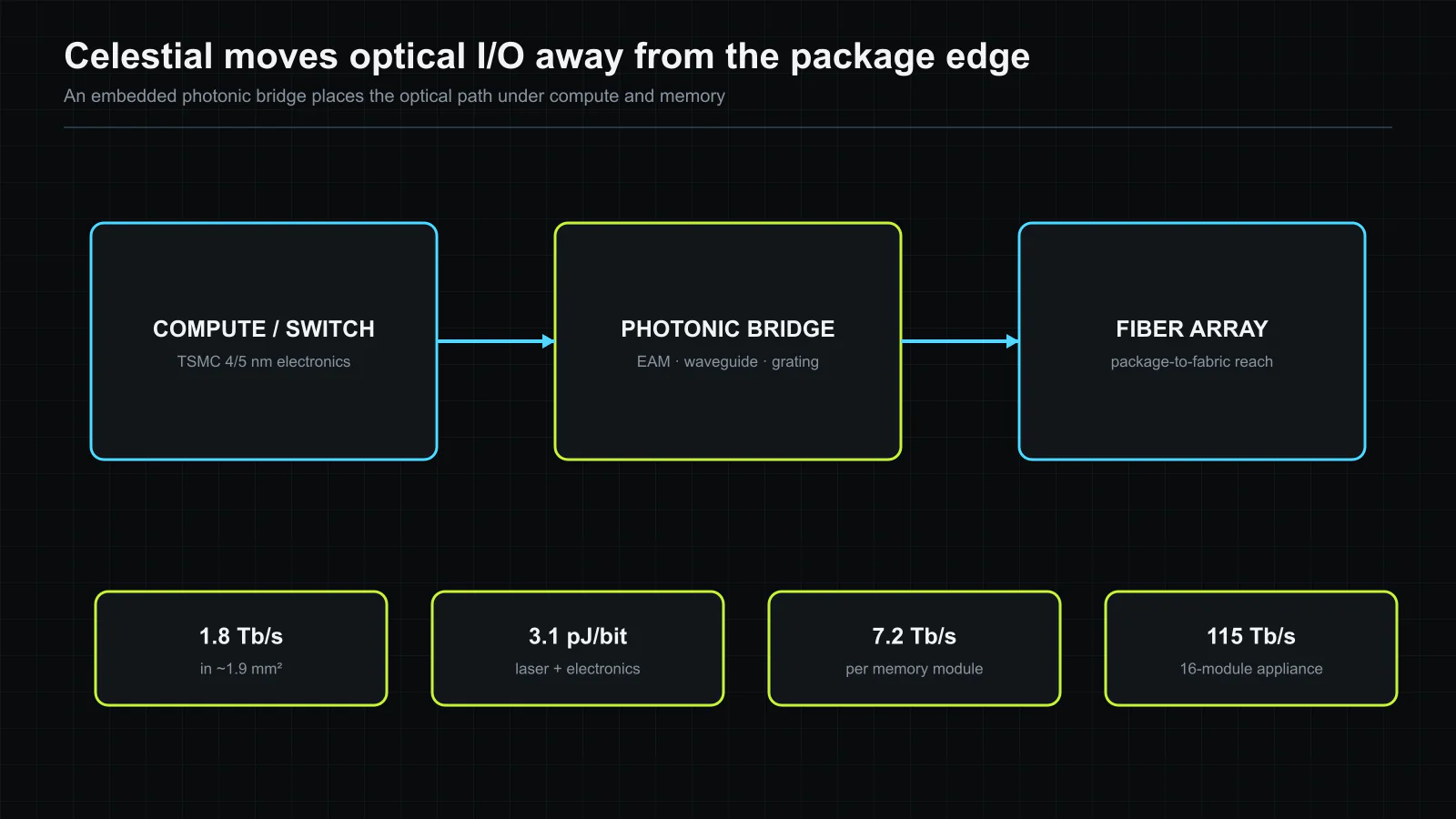
Optical I/O usually approaches a chip from the edge. Pluggable modules sit at the board boundary, and co-packaged optical engines move closer but still consume package shoreline. That edge must also serve HBM, DDR and electrical die-to-die links. Celestial AI’s Hot Chips 2025 presentation proposes a different geometry: put the photonic waveguides and conversion macros in a bridge or interposer that extends under the compute or switch die[1]. Optical reach then begins inside the package instead of at its perimeter.
Celestial calls the link PFLink and the embedded bridge OMIB. A 4/5 nm electrical IC contains drivers, receivers, SerDes and link management. The photonic layer carries electro-absorption modulators, photodiodes, waveguides and grating couplers. An external laser supplies light, keeping the heat-sensitive laser away from the high-power package.
The reason to examine this geometry is that it changes the scarce resource from package edge length to an active substrate under the dies. The relevant decision is whether the recovered shoreline remains valuable after laser power, thermal control, package yield, and memory semantics are counted. This review keeps the measured macro and link results separate from the larger memory-fabric system that the company projects.
The shoreline is the resource being recovered
Electrical bandwidth scales poorly with distance because equalization and SerDes power rise as the channel grows. Conventional co-packaged optics improves reach, but optical engines arrayed along the die edge still limit how much bandwidth can enter the chip. Celestial’s embedded approach moves optical injection points inward and leaves edge length available for memory interfaces or other PHYs.
The company reports 1.8 Tb/s of link bandwidth in about 1.9 mm² for a tested analog macro. Laser energy is stated as 0.7 pJ/bit and electronics as 2.4 pJ/bit, for 3.1 pJ/bit before broader system overhead. A WDM link measured pre-FEC bit-error rate below 10^-8[1]. These are silicon and link measurements, not only package renderings.
The modulator choice is about temperature
Embedding photonics near a multi-kilowatt package exposes it to a wide thermal range. Celestial uses electro-absorption modulators (EAMs), which the company describes as broadband and stable over more than an 85°C range with bias control. Ring modulators are compact and efficient but require resonance tracking; Mach-Zehnder devices are broadband but occupy more area. Celestial argues that EAMs provide the density and thermal behavior needed under a compute die.
That claim should be judged at package scale. A macro can survive temperature variation while fiber attach, grating-coupler loss, process spread and many-channel calibration still determine system yield. The presentation states that four electrical-IC tapeouts were completed and shows a full WDM link, but it does not disclose high-volume assembly yield.
A memory module becomes a fabric endpoint
The proposed first-generation module combines a photonic fabric ASIC with HBM3 and DDR5. HBM acts as a write-through cache for up to 2.07 TB of memory, while the module supplies 7.2 Tb/s full-duplex bandwidth at about 200 ns according to the vendor. Sixteen modules form a 2U appliance with 33 TB and a claimed 115 Tb/s switch[1].
These numbers describe a product architecture rather than an independently benchmarked shipping system. The cache policy, workload locality and access distribution will determine whether DDR capacity behaves like HBM to an accelerator. The 200 ns figure also needs a defined measurement boundary before comparison with CXL memory or local HBM.
The useful architectural point survives those caveats. Once optical I/O begins under the die, memory, accelerators and switches can share one package-to-package link technology over millimeters and meters. This reduces the number of electrical-to-optical boundaries, but increases dependence on advanced packaging and fiber attach.
From link evidence to manufacturing evidence
Celestial has presented measured macros, WDM behavior and several tapeouts. The next evidence should show multi-channel package yield, aging under realistic thermal cycles, laser-wall-plug power and application performance through the memory hierarchy. Appliance availability, cost and serviceability will determine whether the recovered shoreline compensates for optical assembly complexity.
The larger conclusion is that optics is moving from a network component into a packaging primitive. Celestial’s design is one of the clearest expressions of that direction because it treats the photonic layer as an interposer resource. If manufacturing follows the electrical results, the package edge stops being the hard boundary between compute and fabric.
Electro-absorption changes the optical building block
Celestial AI emphasizes electro-absorption modulators (EAMs) rather than relying only on microring or Mach-Zehnder modulators. An EAM changes how strongly a material absorbs light under an applied electric field. The device can be compact and driven with a relatively small electrical swing, which is attractive when many lanes must fit beside a large digital die[1]. Its operating range, insertion loss and temperature behavior nevertheless determine how much laser power and control circuitry the system needs.
Microrings offer small area but usually require wavelength alignment as temperature and process vary. Mach-Zehnder structures can be more tolerant in some respects but occupy longer optical paths and may need larger drive energy. An EAM makes a different trade: compact modulation with material and bias constraints. The correct comparison includes driver power, optical loss, thermal stabilization, receiver sensitivity and lane yield, not modulator area alone.
The receiver side is equally important. Photodetectors and electrical front ends must recover data at the target rate under the optical power that remains after fiber, coupler and modulation loss. Adding laser power can close a link budget but increases facility and cooling load. A credible module therefore balances transmitter efficiency, receiver sensitivity and acceptable bit-error rate across temperature and aging.
The optical multi-chip interconnect is a packaging interface
Celestial’s optical multi-chip interconnect bridge places optical I/O close to the compute or memory die while retaining an electrical connection inside the package. This location aims to shorten the high-speed electrical reach that would otherwise consume equalization power and package routing. The bridge is valuable only if its electrical edge, optical edge and mechanical assembly can all be manufactured with adequate yield.
Compatibility with established advanced packaging matters because a new optical fabric cannot require the entire compute package supply chain to be replaced at once. The company presents the bridge as compatible with high-density packaging approaches such as CoWoS[1]. Compatibility should be interpreted as an integration path, not proof that every package stack, thermal lid and assembly line is qualified.
Fiber attach is a likely yield and serviceability boundary. Hundreds of optical channels need precise alignment, stable coupling loss and a connector scheme that survives assembly and field handling. Passive alignment can reduce cost if the mechanical tolerances are sufficient; active alignment can improve coupling but adds time and equipment. Module-level optical test before final assembly is essential because scrapping an expensive compute package for one failed optical lane would erase much of the economic benefit.
Memory traffic gives the fabric a concrete workload
The Photonic Fabric module combines an optical interface with memory resources, including HBM and external DDR in the disclosed architecture[1]. This makes the device more than an optical cable endpoint. It can place a memory or data-movement function behind the optical link, allowing a compute die to reach capacity without traversing a conventional electrical switch hierarchy in the same way.
The hierarchy still needs software semantics. HBM offers high local bandwidth at limited capacity, while DDR expands capacity with different latency and energy. A controller must decide what data is cached or staged, maintain consistency and expose failures. Optical bandwidth does not make a remote memory access equivalent to a local HBM access; serialization, propagation, protocol and queuing remain.
Workload benefit depends on reuse and transfer size. Large sequential model tensors can amortize setup and use wide links efficiently. Fine-grained dependent accesses may remain latency-limited. Evaluation should therefore include end-to-end application phases and miss behavior rather than only a streaming link test. The module’s architecture is most compelling when software can batch or predict movement across the optical boundary.
Measured, integrated and projected numbers must stay separate
Hot Chips presentations often combine silicon measurements, module demonstrations and road-map projections. Each has a different evidence level. A measured lane can establish modulation and receiver operation. An assembled module can establish integration across many lanes. A projected system bandwidth multiplies lane rate by a planned count and assumes yield, laser and thermal budgets that may not yet be demonstrated simultaneously.
The same distinction applies to energy per bit. Device-level energy can omit off-chip laser, control loops, clocking, retiming and cooling. Package-level electrical power may omit the wall-plug efficiency of the laser source. Facility comparisons need all of these terms and should state whether energy is measured at typical traffic, full utilization or idle. Optical systems can save distance-dependent electrical equalization while adding relatively traffic-independent laser power.
Our interpretation therefore avoids converting one impressive component number into a datacenter claim. The Hot Chips material establishes an industrial integration direction and provides component and module evidence. Product qualification requires lane distributions, bit-error rate over temperature, total wall power and manufacturing yield at the intended channel count.
The fabric competes with an improving electrical baseline
Optical I/O does not enter a static market. Copper SerDes, package substrates, retimers and co-packaged electrical switches continue to improve. For short reaches, electrical links benefit from mature assembly, low idle power and straightforward test. Optics becomes attractive when distance, edge density or equalization energy grows faster than the cost of optical conversion.
The crossover should be measured for a defined reach and topology. A link from one die edge to another package is different from a board, rack or row connection. The saved retimers and switch stages belong in the comparison, as do fiber management, laser redundancy and repair. A module can have a superior link budget yet lose at system level if connector service or spare strategy is expensive.
Celestial AI’s contribution is to treat photonics as a package-scale fabric interface that can sit beside compute and memory, not as a standalone transceiver at the rack edge. That placement could change where memory and accelerator pools are built. The remaining work is industrial: repeatable fiber attach, multi-lane yield, thermal co-design, software memory management and total energy under useful traffic. Those items will decide whether the photonic bridge becomes infrastructure rather than a specialized module.
Source and copyright notice
This article is an independent editorial summary of Celestial AI’s official Hot Chips 2025 presentation. All measurements and projections are attributed to the company and restated in our own words. No slide, product rendering, table or source figure is reproduced. The explanatory figure was created specifically for this article. The source presentation is (c) Celestial AI 2025, all rights reserved.