UCIe defines a short electrical connection between chiplets in a package. AI scale-up fabrics need similar semantics across longer distances, where copper loses reach and pluggable optics add power and latency. Ayar Labs’ Hot Chips 2025 presentation inserts a retimer at that boundary: the host sees UCIe-S, while the chiplet converts the traffic into wavelength-multiplexed optical lanes over single-mode fiber[1].
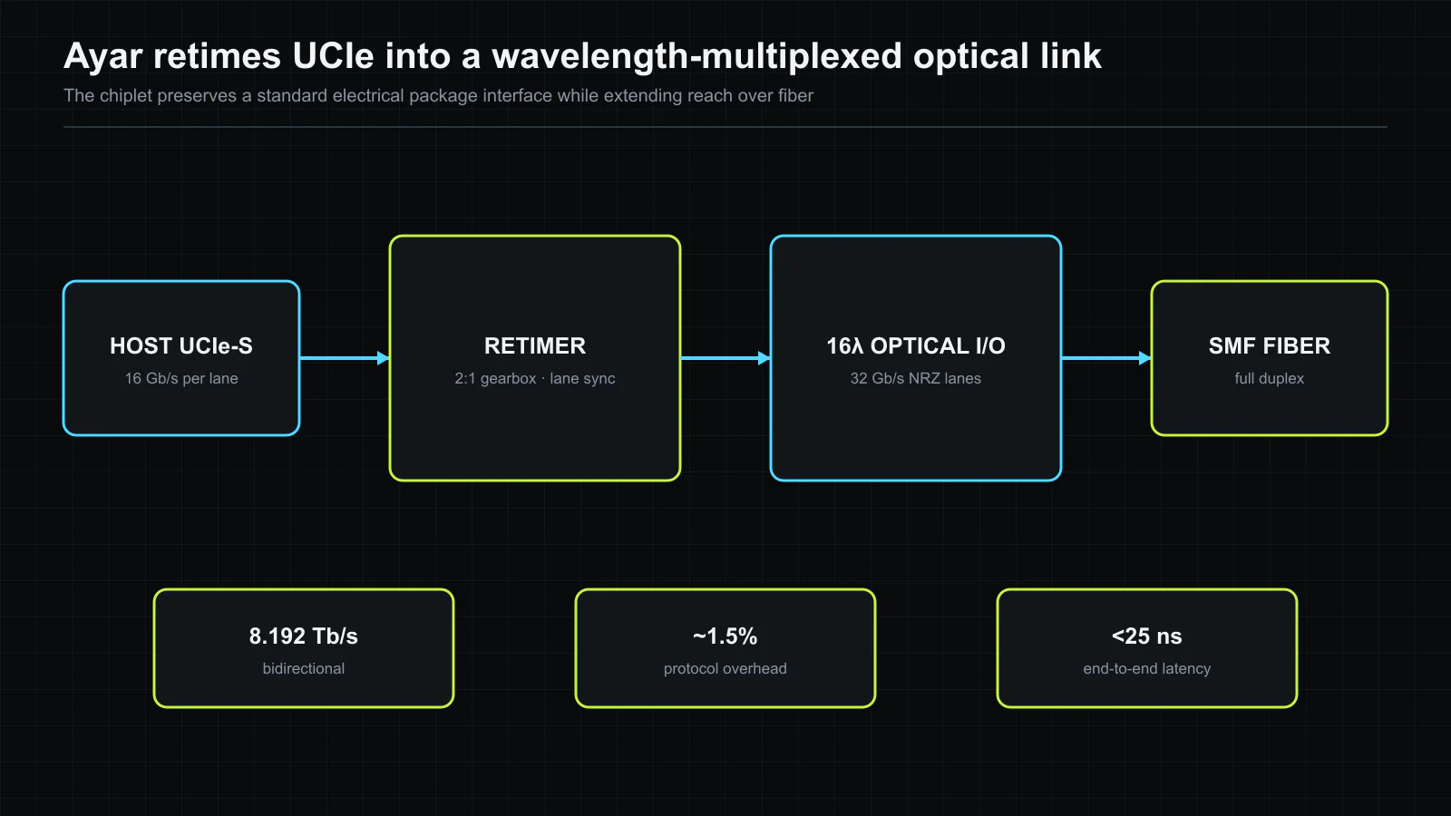
The reported TeraPHY chiplet supports sixteen UCIe modules. Each module carries 512 Gb/s bidirectionally at 16 Gb/s per UCIe lane, producing 8.192 Tb/s aggregate bidirectional bandwidth. Eight optical ports each contain sixteen transmit and sixteen receive lanes at 32 Gb/s NRZ. A SuperNova external laser supplies sixteen wavelengths.
Those figures make the link credible, not the fabric complete. The system decision is whether a standards-facing retimer can extend package semantics without importing the power, latency, and failure model of a conventional network. This review separates measured link evidence from the switching, coherence, thermal, and serviceability work that still sits above it.
Retiming is more than electrical conversion
The chiplet uses a 2:1 gearbox because the electrical UCIe lane and optical lane operate at different rates. It also carries UCIe valid signaling, aligns optical lanes, compensates frequency offset between chiplets and transports sideband or management messages. Ayar reports about 1.5% bandwidth overhead for this adaptation[1].
These functions are essential for a standard interface. A raw optical PHY could move bits but would leave the host to reconstruct lane alignment and protocol state. The retimer preserves the UCIe boundary, allowing a package designer to treat optics as a reach extension rather than a new network interface.
The measurements target system concerns
Ayar reports a five-day error-free test across all sixteen UCIe modules. In a separate end-to-end optical setup, full-duplex traffic remained error-free at every observation point for more than ten hours, with end-to-end latency below 25 ns[1]. Link-margin testing across 306 observations found more than 5 dB after a firmware calibration bug was corrected.
Thermal testing is especially relevant near accelerators. The company applied a 50°C change at 5°C per minute, and reports that most links remained error-free with no bit-error dependence on temperature. An emulated wavelength sweep corresponding to as much as 800°C per second also completed without errors, demonstrating that the tuning loop can follow short transients. Emulation is not identical to heating a packaged system at that rate, so the result validates control response rather than full-package reliability.
The presentation also reveals the operational layer. A firmware bug in transmitter IQ calibration reduced margin until corrected. Optical I/O therefore inherits software lifecycle requirements: initialization code, monitoring and field updates can affect physical-link reliability.
What 8 Tb/s does and does not establish
The chiplet demonstrates that a standard package interface can be extended over fiber at multi-terabit bandwidth and low measured latency. That result addresses a concrete scale-up gap between electrical die-to-die links and network optics. It does not by itself specify a complete fabric. Switching, routing, coherence, collective behavior and failure containment sit above the retimer.
System energy also includes the external laser, thermal tuning, fiber coupling and host UCIe PHYs. The Hot Chips deck focuses on connectivity and validation rather than a complete pJ/bit comparison at the wall. Manufacturing yield for sixteen-wavelength microrings and fiber attachment must be measured across production volume.
The strongest interpretation is therefore architectural. UCIe can remain the package-facing contract while optics changes the reach. If qualification and assembly scale, accelerator and switch vendors can add rack-level optical connectivity without exposing a proprietary optical protocol to the host die. The retimer becomes the seam between an open electrical standard and a photonic fabric.
UCIe makes the electrical edge explicit
The chiplet presents a UCIe-facing electrical interface to the host package and an optical interface to the fabric. UCIe matters because it defines a standardized die-to-die attachment rather than requiring every accelerator vendor to design a proprietary electrical protocol for the optical engine. The optical retimer can then become a package component with a clearer integration contract[1].
Standardization does not eliminate implementation choices. Lane count, lane rate, package channel loss, clocking and protocol mode determine the electrical energy and area. A UCIe-compliant boundary also needs link training, error handling and sideband management. The host must know whether a failure belongs to the local die-to-die link, the retimer, the laser path or the remote endpoint.
The module arithmetic should therefore distinguish raw and usable bandwidth. Multiplying lanes by symbol rate yields a physical figure, while encoding, framing, flow control and retry reduce payload bandwidth. Full-duplex totals can also be mistaken for one-direction throughput. A system claim should state direction, protocol efficiency and the number of optical ports that operated simultaneously.
Retiming creates two clock and fault domains
An optical retimer terminates the local electrical link and launches a new optical link rather than behaving as a passive medium converter. This separation can refresh signal integrity and extend reach, but it introduces buffering, clock recovery and fault translation. Latency includes the electrical receiver, protocol handling, optical transmitter, remote receiver and the corresponding return path for control.
The design uses a lightweight multi-module protocol and sideband mechanisms to coordinate endpoints[1]. Such control paths are easy to overlook in a bandwidth diagram. They handle discovery, link state, resets and management when the high-speed data path is unavailable. Their reliability determines whether a failed optical lane can be isolated and retrained without resetting the entire accelerator package.
Flow control must span the domains without creating deadlock. If the optical side pauses while the UCIe side continues sending, buffers can fill. If backpressure is too conservative, a long optical path remains underused. Credit depth and retry policy need to cover propagation delay, packet size and the number of outstanding transactions. These are system-level choices even when the retimer implements them in hardware.
Laser location changes energy and serviceability
A photonic I/O chiplet needs a light source. The laser can be placed near the package or provided remotely and distributed to several engines. A remote laser can keep heat and laser replacement away from the expensive compute package, and it may allow sharing or redundancy. It also adds fiber paths, connectors and optical distribution loss.
Laser efficiency belongs in every energy-per-bit comparison. Electrical energy measured on the retimer does not include the wall power needed to create the optical carriers. Control circuits that stabilize wavelength or power also consume energy at idle. Conversely, one laser can serve many active lanes, so assigning its entire power to a lightly used link can overstate the cost. Reporting both full-load and utilization-weighted energy avoids either error.
Service design is important because lasers age differently from digital silicon. A replaceable external source can improve maintainability if the distribution network has isolation and monitoring. Redundant lasers can preserve service, but failover must not violate optical power limits or create a long interruption. Optical telemetry should expose launch power and receive margin before a link reaches the error threshold.
Thermal design links the optical and electrical sides
Placing the chiplet beside a high-power accelerator shortens the electrical path and exposes photonics to a difficult temperature environment. Modulator efficiency, detector response and optical coupling can shift with temperature, while the retimer’s SerDes and protocol logic add their own heat. The thermal solution must keep both compute and optics within specification without blocking fiber access.
A package-level demonstration should map performance across realistic temperature gradients, not only a controlled bench temperature. The lanes nearest a hot compute die may have different margin from those near the package edge. Dynamic accelerator load can change temperature faster than a slow calibration loop responds. Results should include bit-error rate before and after correction, retraining frequency and total cooling power.
Mechanical stress also matters. Package warpage and thermal cycling can change coupler alignment or micro-bump resistance. High-bandwidth operation at room temperature is the first step; qualification requires cycling, vibration where applicable, and accelerated aging. These tests decide whether optical I/O can share the lifetime expectations of an accelerator module.
An optical link is not yet an optical fabric
The Ayar Labs chiplet solves an endpoint problem: convert a standardized local interface into multiple high-bandwidth optical connections. A scale-up fabric still needs topology, switching or circuit assignment, routing, congestion control, collective algorithms and management. Direct point-to-point links can serve a small group, while larger systems need a method to connect more endpoints than one package can reach directly.
Topology affects the apparent benefit. A retimer can bypass a power-hungry electrical reach or switch stage, but an optical fabric may add optical circuit switches and scheduling delay. Failure recovery must coordinate the chiplet with the broader path. Thus, endpoint bandwidth should not be multiplied by package count and called bisection bandwidth without specifying connectivity and oversubscription.
The strongest Hot Chips evidence is that UCIe, protocol control and optical lanes were integrated into one retimer chiplet and exercised as a link. The next evidence should show many chiplets operating simultaneously through a defined topology, including link failures, sustained traffic and application collectives. That will reveal whether control, laser and thermal overhead remain bounded at rack scale.
Where the design can create system value
The chiplet is attractive when an accelerator vendor wants optical reach without embedding a full photonics process in the compute die. A standardized die-to-die edge can let each side use a process suited to its function. It may also permit optical I/O generations to change independently from the accelerator, provided the package and protocol remain compatible.
This modularity has an economic condition. The retimer, fiber attach, laser and package area must cost less than the electrical components, board complexity and power they replace. Yield should be separable so a failed optical chiplet does not discard a good compute die. Pre-bond test, known-good-die strategy and field diagnostics are therefore as important as peak lane rate.
Ayar Labs has demonstrated a credible bridge between an emerging chiplet standard and optical scale-up connectivity. The public material establishes integration and link operation, not a universal fabric benchmark. Its commercial advantage will depend on total wall energy, multi-lane yield, thermal margin, manageability and the network built above the endpoint.
Source and copyright notice
This article is an independent editorial summary of Ayar Labs’ official Hot Chips 2025 presentation and the referenced UCIe interface specification. We restated the architecture, tests and limitations in our own words. No source slide, eye diagram, table or figure is reproduced. The explanatory figure was created specifically for this article. The presentation is (c) Ayar Labs 2025, and the UCIe specification is subject to the consortium’s terms.