SmartNIC acceleration is easiest when the working set fits on the card. Ordered key-value stores violate that assumption. Their B-trees can occupy hundreds of gigabytes in host DRAM, while an FPGA has limited SRAM and on-board memory. If the FPGA follows every tree pointer over PCIe, the accelerator can spend more time waiting for the host than executing comparisons.
Honeycomb takes that difficult split deliberately[1]. GET and SCAN run on an FPGA SmartNIC and bypass the host CPU. PUT, UPDATE, and DELETE remain on CPU cores. The complete B-tree stays in host DRAM so capacity scales with server memory and the FPGA image remains manageable. The system then treats PCIe as a memory-hierarchy boundary that must be cached, parallelized, and synchronized.
The evaluated FPGA connects through two PCIe Gen3 ×8 links. The authors measure 13 GB/s peak throughput and more than 1 microsecond of access latency depending on load, compared with up to 64 GB/s and roughly an order of magnitude lower latency from the CPU to DRAM. Honeycomb succeeds not by making PCIe fast, but by ensuring that most requests do not wait for one serialized PCIe tree walk.
A B-tree split by operation, not by capacity
Read requests arrive directly from the network subsystem through an RDMA engine with custom GET and SCAN commands. The FPGA’s B-tree accelerator parses the command, traverses cached or host-resident nodes, and returns a reply without scheduling a server thread. Writes arrive through the normal service path and modify the tree on the CPU. This split matches read-dominated workloads and keeps complex allocation and structural changes in software.
The root occupies on-chip SRAM, and the card’s DRAM holds frequently referenced nodes from upper tree levels. Leaves and the complete authoritative structure remain in host memory. A page table on the FPGA maps stable logical node identifiers to physical host addresses. When the CPU replaces or merges a node, it can change the mapping atomically rather than forcing the FPGA to chase a partially updated pointer.
Large B-tree nodes improve fan-out and reduce tree depth, but fetching a whole node over PCIe wastes bandwidth when one key range is relevant. Honeycomb adds shortcuts: sorted keys and offsets identify the segment that may contain the target. The FPGA fetches only that portion. This preserves the shallow tree of a large node while approaching the transfer size of a smaller node.
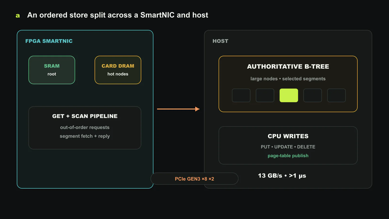
The cache also uses both available paths. Requests that miss on-chip SRAM may use on-board DRAM, but if that channel is saturated while PCIe has bandwidth, a dynamic load balancer can fetch a cached node from host memory instead. The fastest location is not fixed; it depends on instantaneous queueing in the memory subsystem.
Concurrency hides a microsecond path
A serial B-tree walk turns every PCIe latency into exposed request time. Honeycomb issues many independent requests and executes them out of order so one transaction can progress while another waits. The FPGA contains separate stages for traversal, DMA, comparison, and reply. Deep queues are useful because PCIe bandwidth can be filled only with enough outstanding work.
This choice changes latency behavior. One request may not become faster, but aggregate throughput rises as independent misses overlap. The architecture is therefore best suited to services with enough request concurrency. A low-rate control operation that requires strict serial dependence would still see the full PCIe latency.
Range scans benefit from offload because the FPGA can follow adjacent leaf data and stream results without repeated client round trips. A one-sided RDMA client normally needs at least one read to locate a node and another to fetch variable-sized data, plus client caching to avoid repeated traversal. Honeycomb keeps traversal next to the server’s network interface while preserving a large host-memory store.
Wait-free reads across CPU and FPGA
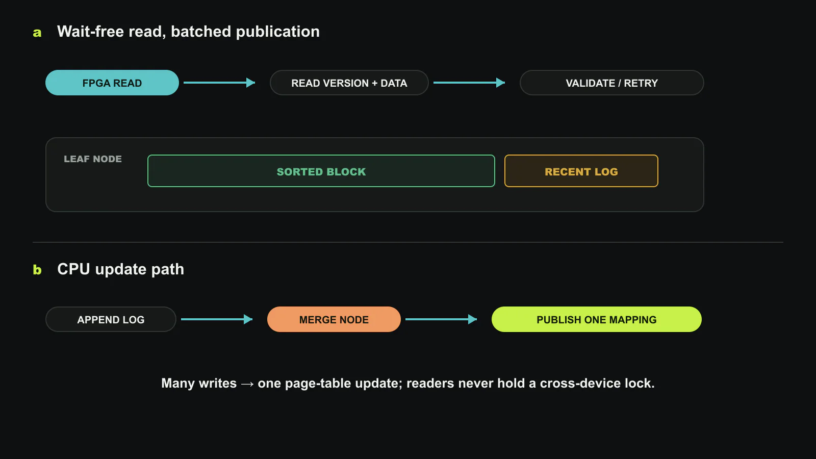
The harder problem is correctness. The CPU changes nodes while the FPGA reads them over PCIe. Taking a lock on every read would serialize the accelerator and require cross-device synchronization. Honeycomb instead makes GET and SCAN wait-free. A leaf has a sorted block and a small log block containing recent updates. Readers inspect a stable version and verify metadata before accepting the result. If a concurrent change invalidates the view, the request retries rather than blocking the writer.
The CPU batches structural synchronization. Updates accumulate in the log, and a merge creates a new sorted node. The page table mapping changes after the new state is ready. One mapping update represents many writes, reducing PCIe control traffic. Stable logical identifiers allow the FPGA to continue referencing a node while physical host addresses change.
Linearizable scans require more than per-key consistency. A scan must represent one legal point in the global operation order even when it crosses leaves. Honeycomb’s versioning and update protocol ensure that a scan either sees a compatible set of nodes or retries. This is a substantial part of the contribution: offloading a lookup that sometimes returns stale data would be much simpler but unsuitable for an ordered storage service.
Throughput and cost under read-heavy workloads
Honeycomb is compared with a leading ordered key-value system on YCSB-style workloads and scan-heavy mixes inspired by cloud storage. In the read-dominated YCSB cases, its throughput is no less than 1.8× the baseline; scan-heavy mixes exceed 2×. Under a uniform key distribution with inserts and brief range scans, the paper reports 1.2× at a 50% read share and more than 2.3× once reads account for at least 80%.
The trend follows the operation split. As the write share grows, more work remains on the CPU and synchronization activity increases. Read and scan traffic can bypass the CPU and use FPGA parallelism, so the accelerator’s return rises with read ratio. This is not a general acceleration factor for all key-value workloads.
Cost-performance improves by at least 1.5× for the main read-heavy and scan-heavy cases. That denominator matters because an FPGA SmartNIC adds capital cost and power. Higher raw throughput is insufficient if an equivalent number of CPU servers is cheaper. The paper’s cost model supports the evaluated platform, while current pricing and newer CPU or DPU alternatives should be recalculated.
The authors expect PCIe Gen5 and larger FPGA caches to improve results. Their prototype uses Gen3, and Gen5 offers four times the nominal bandwidth. That projection is plausible for bandwidth-bound misses but does not remove fixed traversal dependencies, synchronization, or cost. A faster link may also shift the bottleneck to on-board DRAM, FPGA pipelines, or network rate.
The workload boundary
Honeycomb assumes an ordered, read-dominated in-memory service. Write-heavy workloads receive less benefit because CPU execution and publication dominate. Very small stores that fit on the FPGA could use a simpler fully offloaded design. Extremely large scans may become limited by PCIe and network output regardless of traversal acceleration.
The FPGA image implements a specific B-tree layout and custom network commands. Changing key format, value semantics, compression, or transaction rules requires hardware and software changes. The CPU-FPGA protocol must be maintained across upgrades. Programmability is lower than a CPU-only service, so stable operations and high volume are prerequisites for amortizing development.
Failure recovery is another boundary. The authoritative tree is in host DRAM, but in-flight FPGA requests, cache contents, page-table mappings, and network replies need coordinated reset behavior. A production design must define what happens when the FPGA restarts, a PCIe link fails, or the CPU process crashes during a merge. The performance paper concentrates on normal operation.
PCIe as a co-design boundary
Honeycomb provides a useful rule for SmartNIC projects: do not move the entire data structure merely to avoid PCIe. Keep capacity where it scales, move the operation whose parallelism and CPU cost justify offload, and design the boundary as a hierarchy. Caching reduces crossings, segmentation reduces bytes per crossing, concurrency hides latency, and versioned publication reduces synchronization crossings.
An accelerator proposal should therefore report four quantities: miss traffic over PCIe, outstanding concurrency needed to reach bandwidth, synchronization bytes per update, and the workload read or scan ratio. Peak FPGA logic rate alone says little when the authoritative data is elsewhere.
The deeper result is that a slow boundary can be acceptable when its semantics are controlled. Honeycomb does not claim PCIe is low latency. It arranges the data structure so that the fixed latency is either avoided, amortized, or overlapped, while the CPU remains responsible for the changes that are hardest to implement safely in hardware.
Source and copyright notice
This article is an editorial analysis by Silicon & Systems. It restates the paper’s architecture, evaluation, and limits in our own words. No source sentence, table, or figure is reproduced; all figures were created for this article. The reviewed author version is available on arXiv, and the journal record is available through the IEEE DOI. (c) IEEE 2024.